-

Figure 1.
Overall circuit configuration of proposed WPT system and circuit configuration of the LCC-LCC compensated WPT system for CC charging.
-

Figure 2.
Circuit configuration of the LCC-S compensated WPT system for CV charging.
-
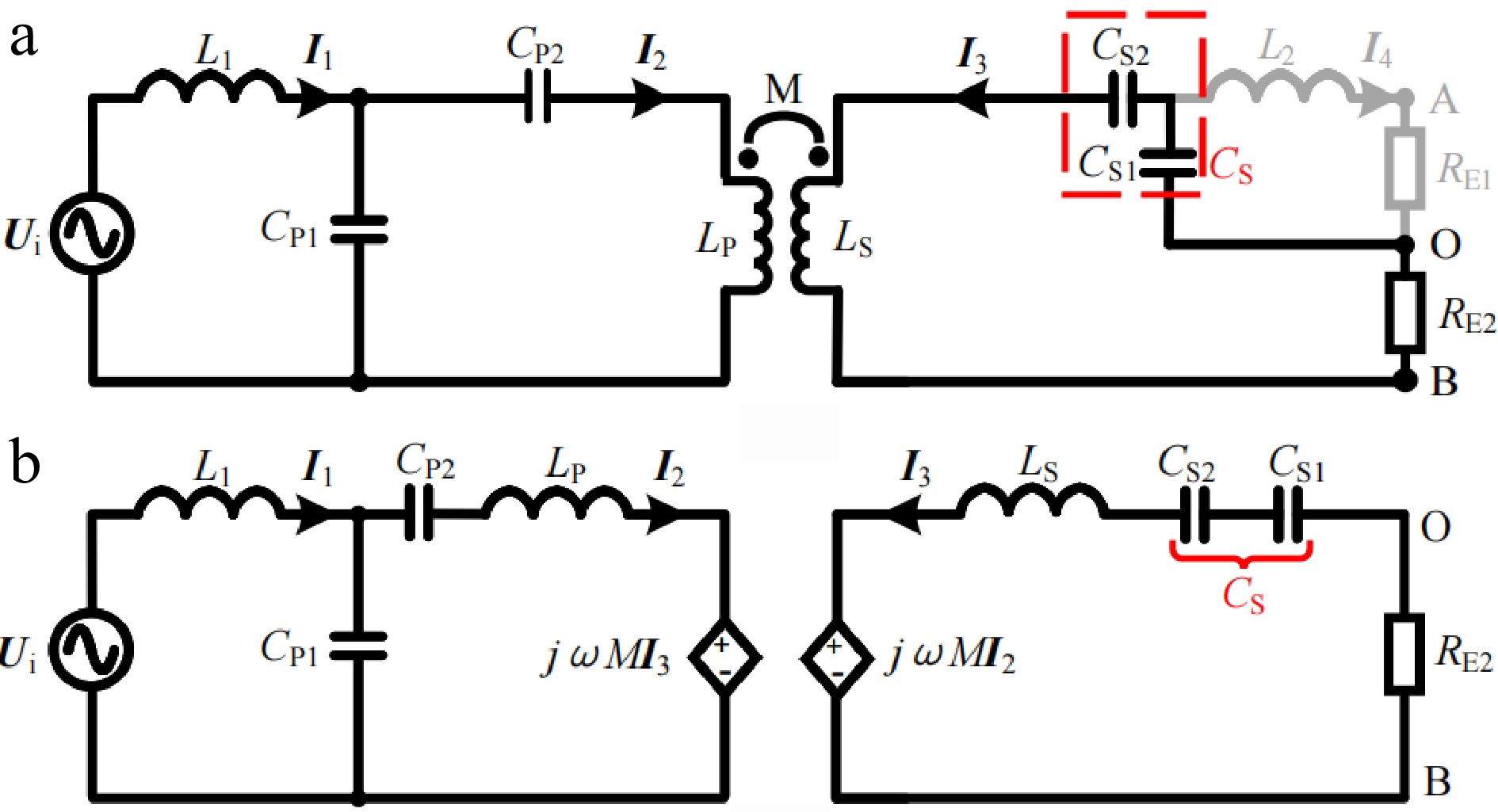
Figure 3.
Simplified circuit diagram and equivalent circuit diagram in CV mode. (a) Simplified circuit diagram. (b) Equivalent circuit diagram.
-
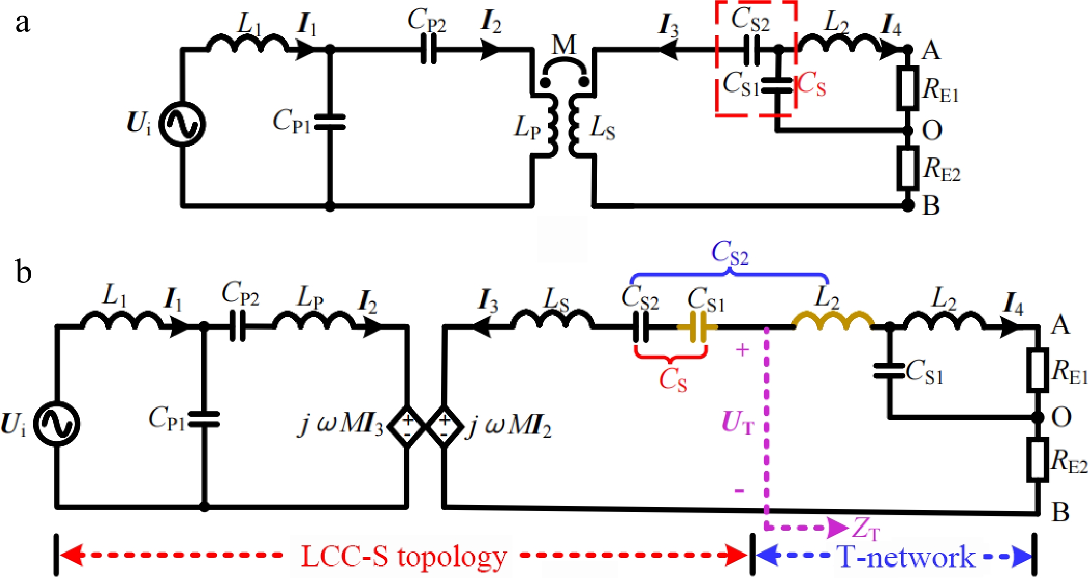
Figure 4.
Simplified circuit diagram and equivalent circuit diagram in CC mode. (a) Simplified circuit diagram. (b) Equivalent circuit diagram.
-
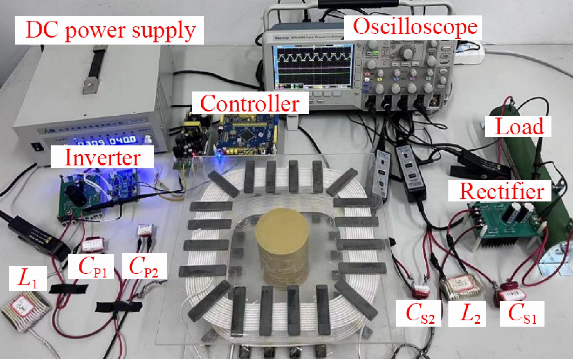
Figure 5.
Experimental prototype.
-
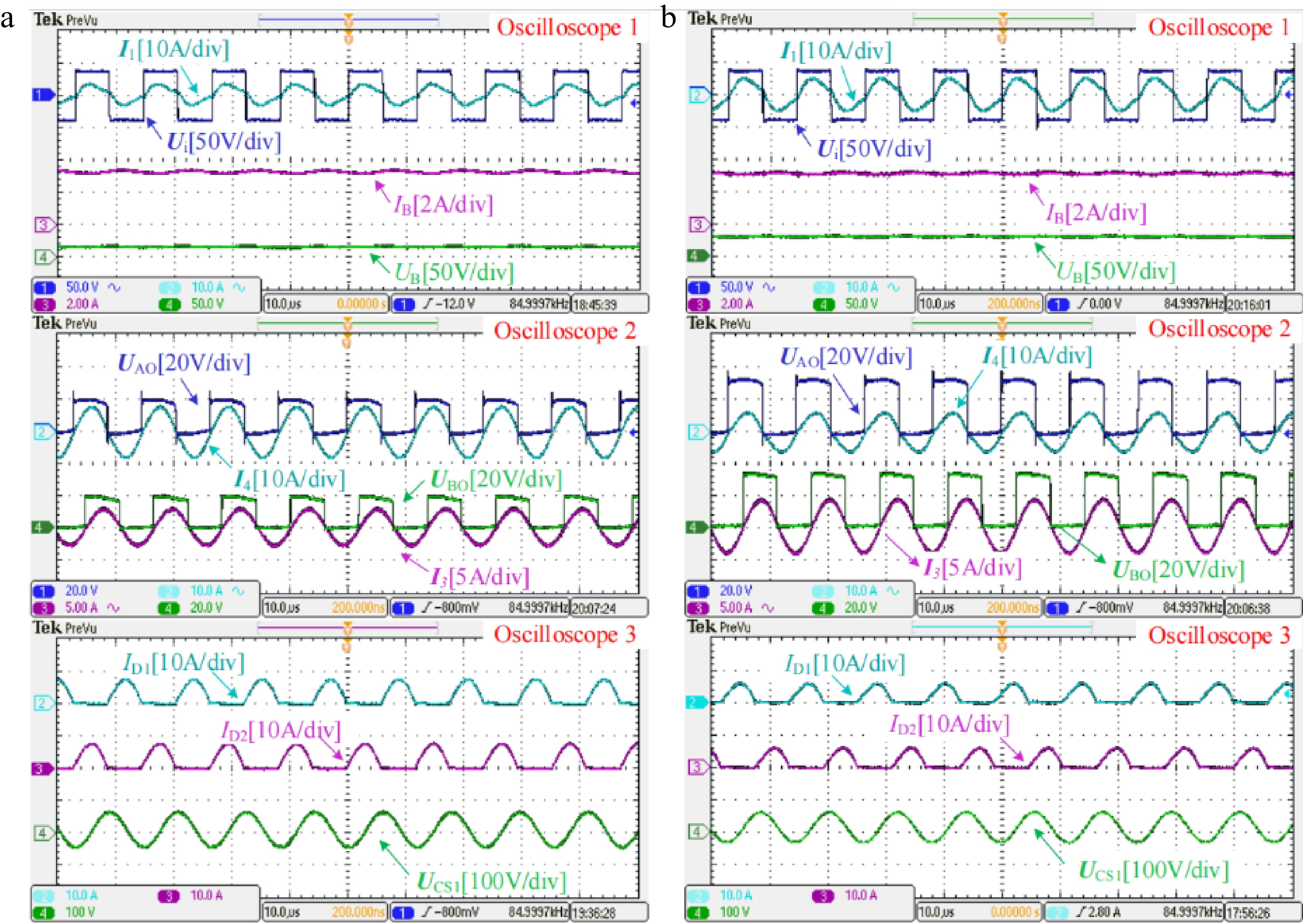
Figure 6.
Measured experimental waveforms in CC mode when the battery equivalent resistance RB is about (a) 5 Ω and (b) 10 Ω, respectively.
-
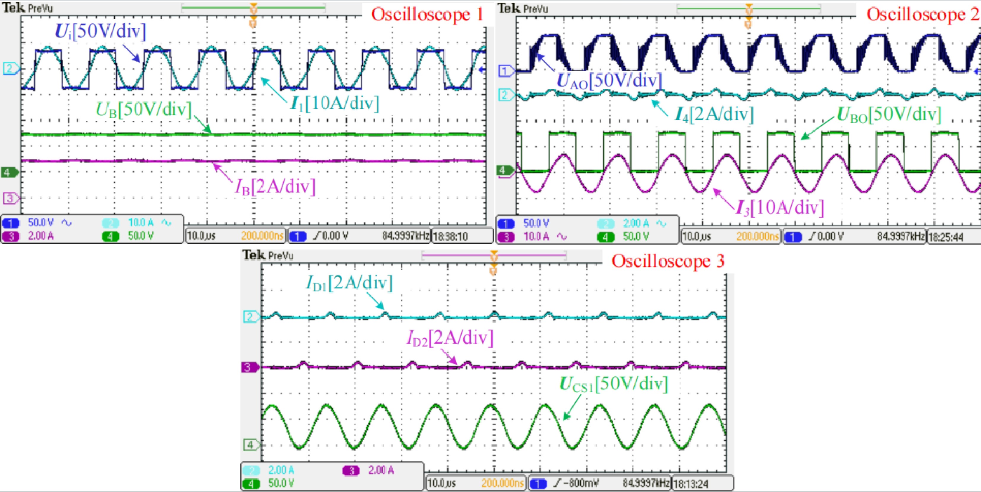
Figure 7.
Measured experimental waveforms at the CC-CV transition point when the battery equivalent resistance RB is about 25 Ω.
-
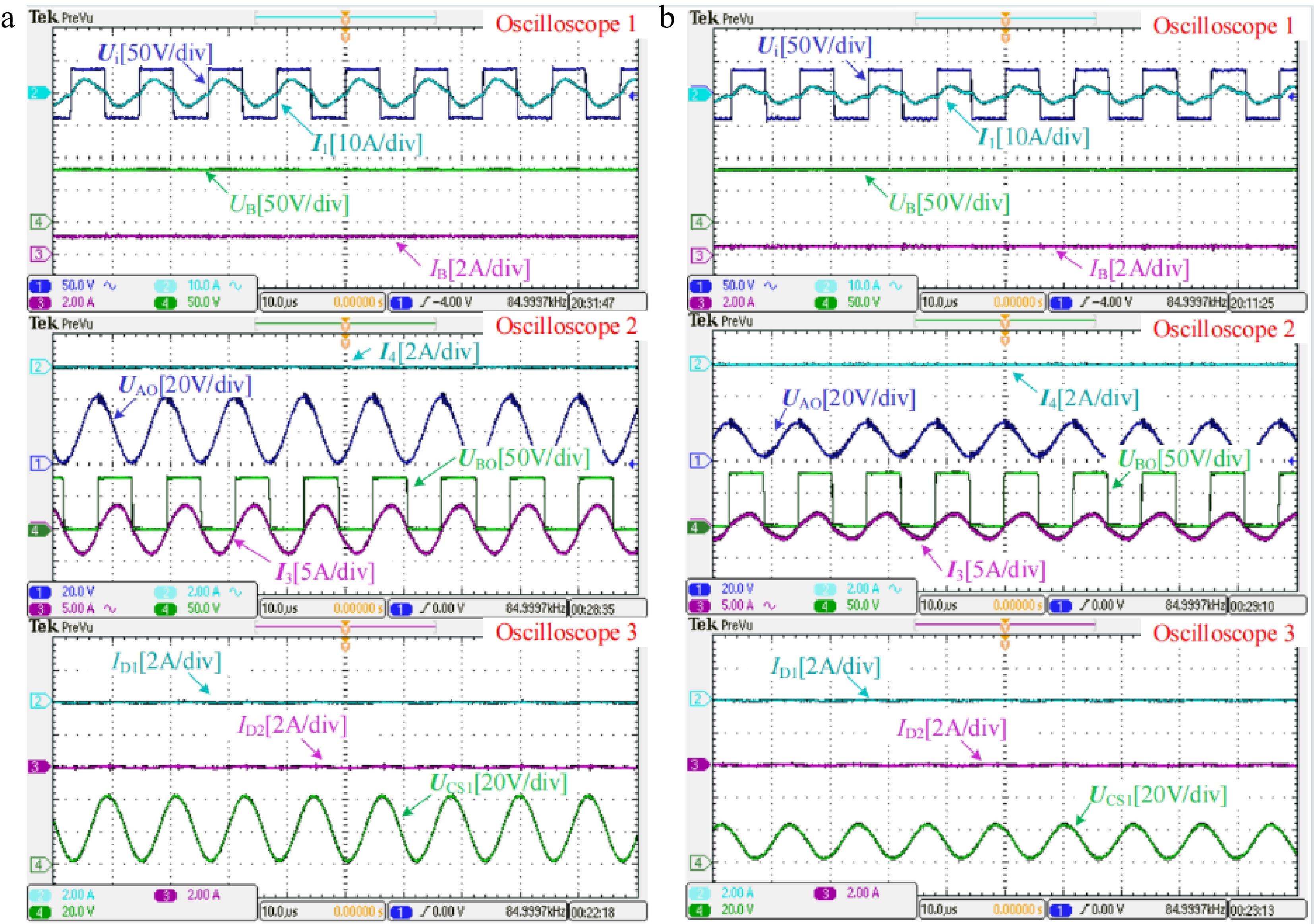
Figure 8.
Measured experimental waveforms in CV mode when the battery equivalent resistance RB is about (a) 70 Ω and (b) 140 Ω, respectively.
-

Figure 9.
Transient results with load step changes (a) from 5 to 10 Ω and (b) from 70 to 140 Ω.
-
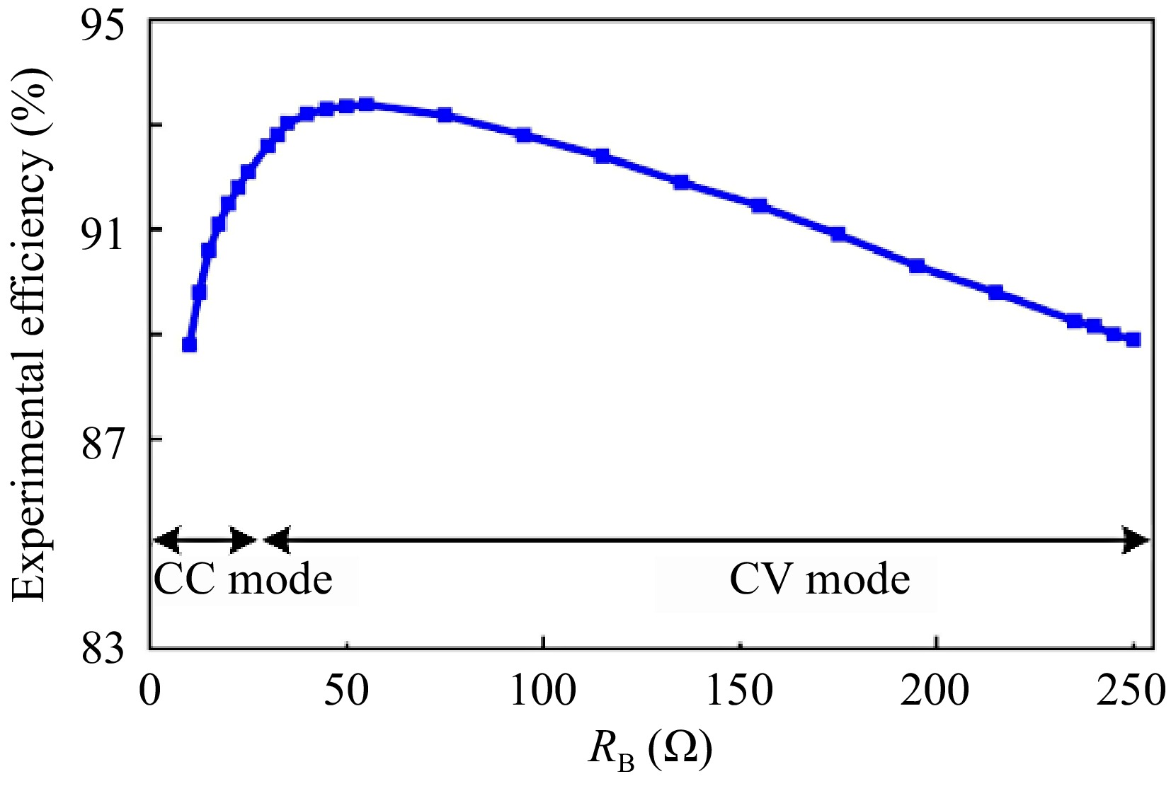
Figure 10.
DC-DC efficiency curve of the proposed system during the whole charging process.
-
Parameters Value Parameters Value Parameters Value UD 40 V LP 100.3 uH CP1 175.4 nF UB 80 V LS 100.1 uH CP2 34.9 nF IB 3.2 A L1 19.8 uH CS1 365.2 nF f 85 kHz L2 9.6 uH CS2 38.8 nF M 20.4 uH RP 0.12 Ω RS 0.1 Ω Table 1.
Specific circuit parameters of the proposed LCC-LCC compensated WPT system.
-
Proposed in Ref. [10−13] Ref. [14−18] This study Method Hybrid topology switching Dual-frequency switching Automatic CC-CV transition Without detection circuits No No Yes Without communication links No No Yes Without open-circuit protection circuits No No Yes Without excess components and switches No Yes Yes Cost High Medium Low Table 2.
System configuration and cost comparison with existing popular methods
Figures
(10)
Tables
(2)