-
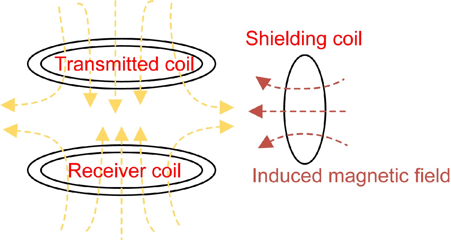
Figure 1.
Schematic diagram of reactive power shielding.
-
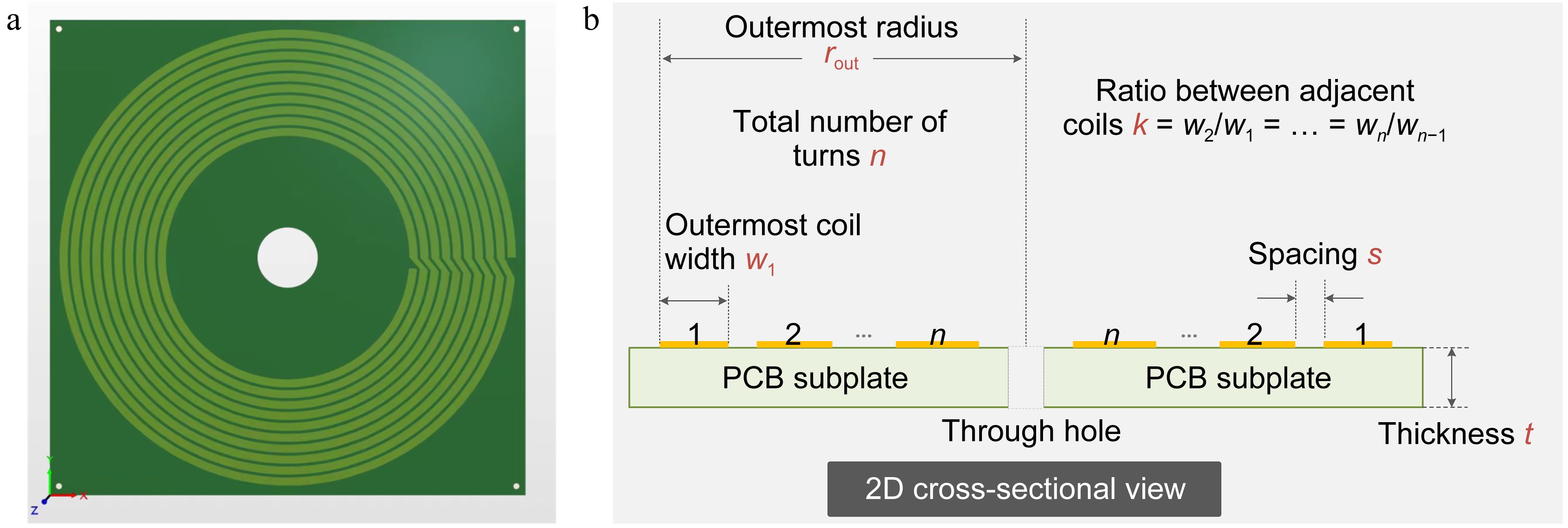
Figure 2.
Diagram of shielding coil and 2D cross-sectional view.
-
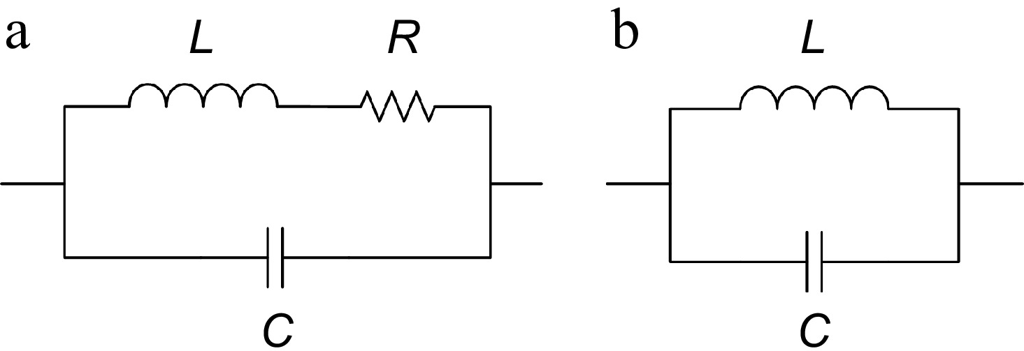
Figure 3.
The equivalent circuit of the shielding coil. (a) Complete equivalent circuit. (b) Simplified equivalent circuit.
-
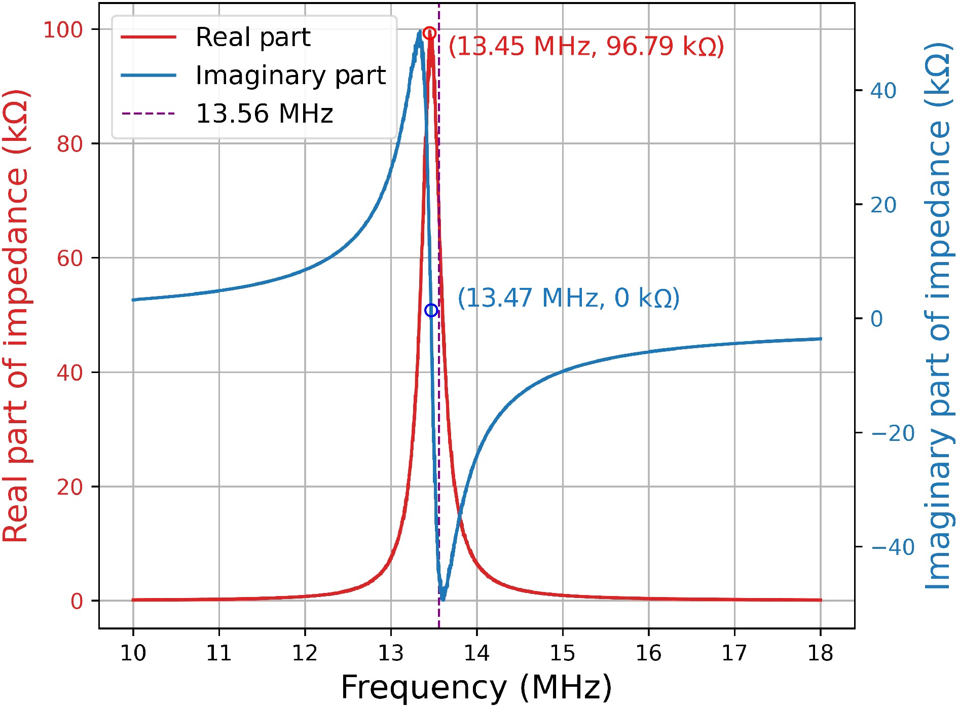
Figure 4.
Impedance of the shielded coil, including the real part and the imaginary part.
-
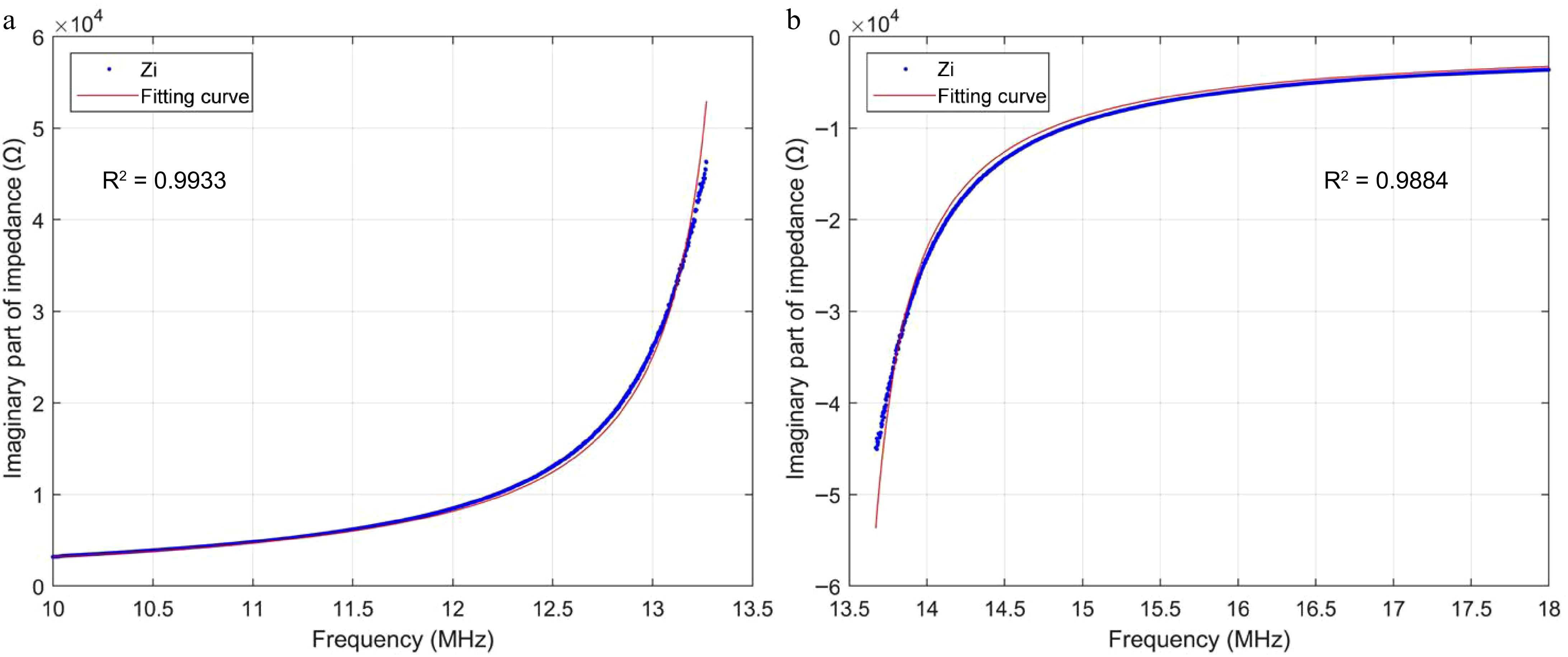
Figure 5.
Curve fitting of the imaginary part of impedance.
-
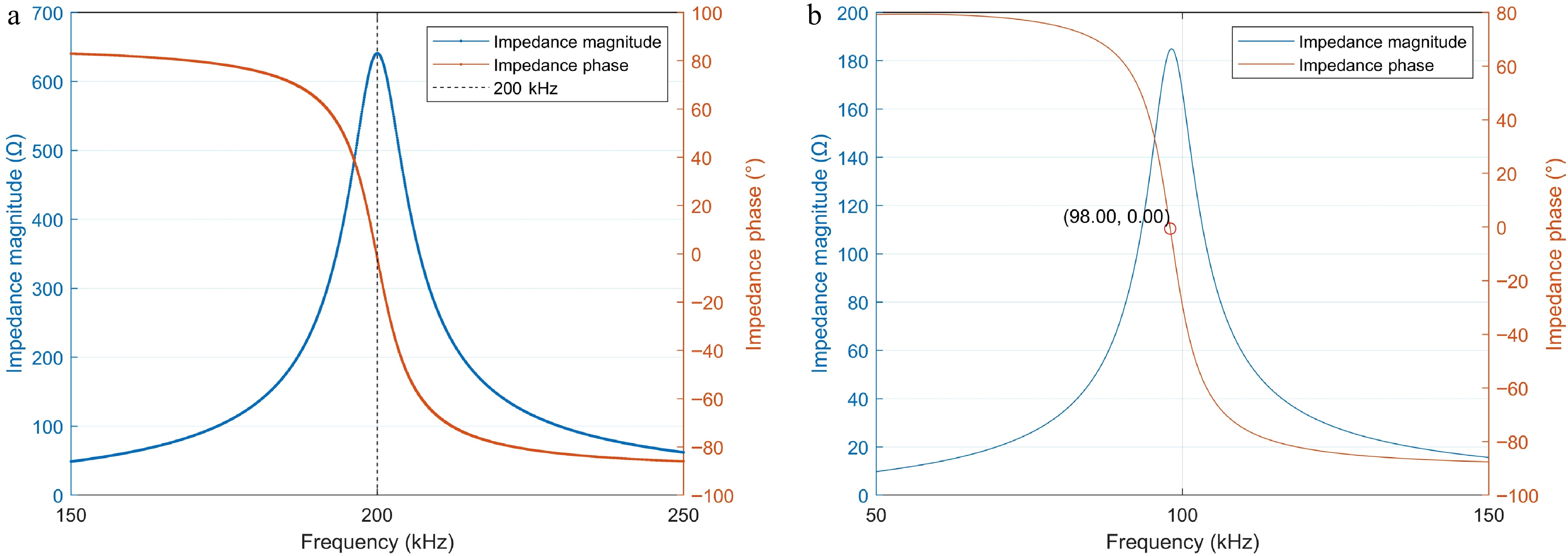
Figure 6.
Magnitude and phase of impedance of the shielding coil. (a) 200 kHz. (b) 100 kHz.
-
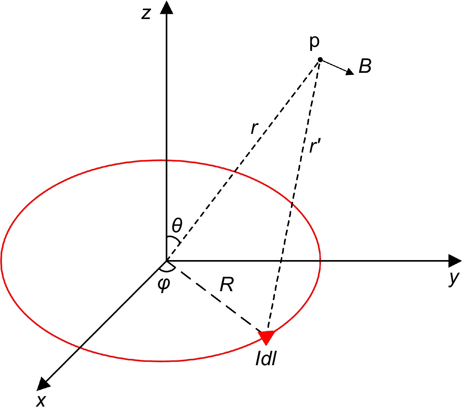
Figure 7.
Coordination system of the small loop current.
-
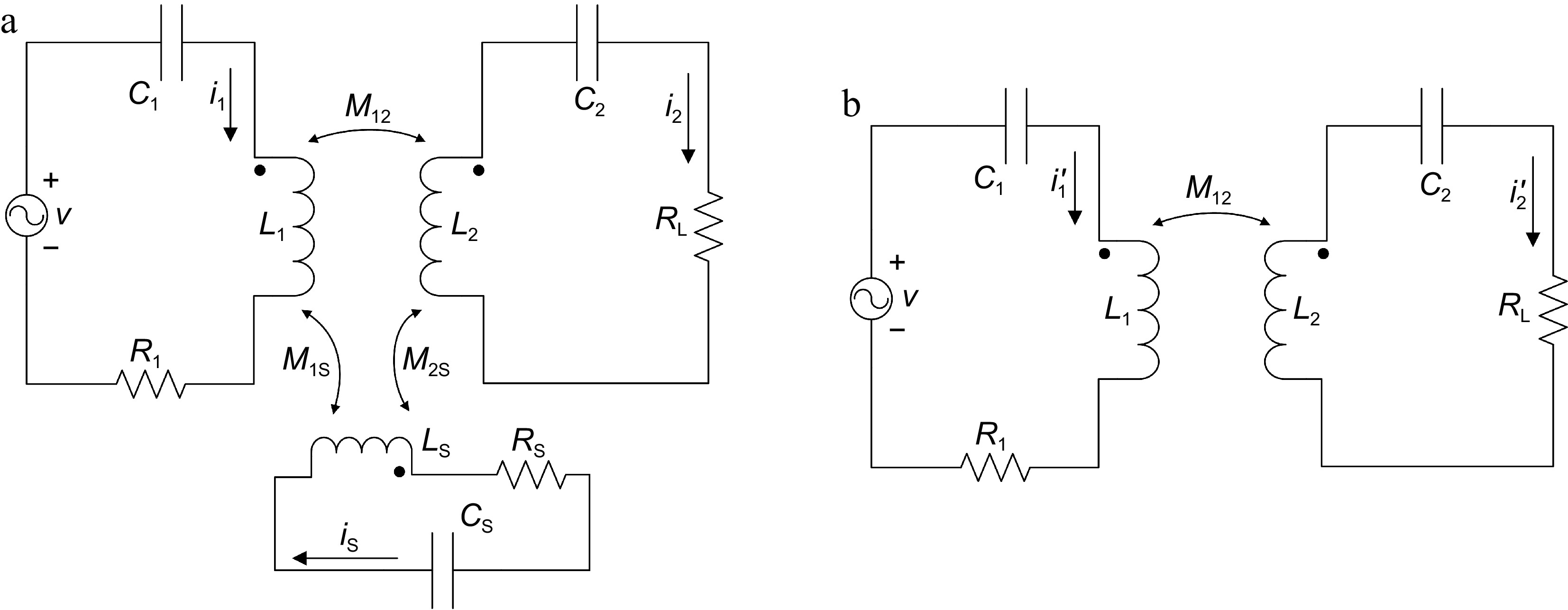
Figure 8.
Circuit structure of the WPT system: (a) with a shielding coil, (b) without a shielding coil.
-
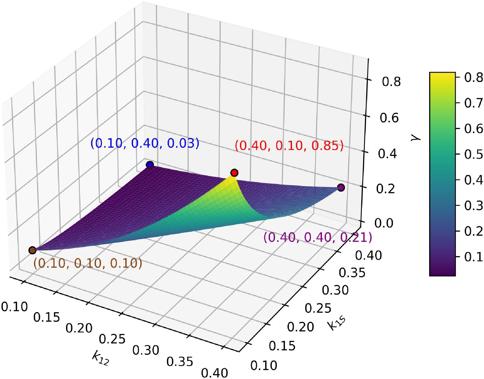
Figure 9.
γ in different k12 and k1S.
-
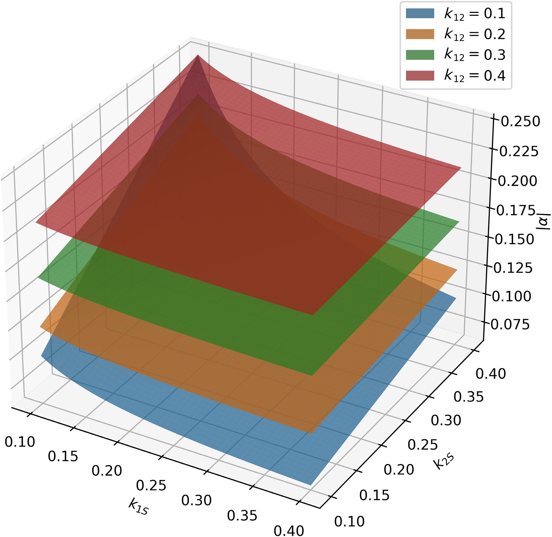
Figure 10.
$\left| \alpha \right|$ -
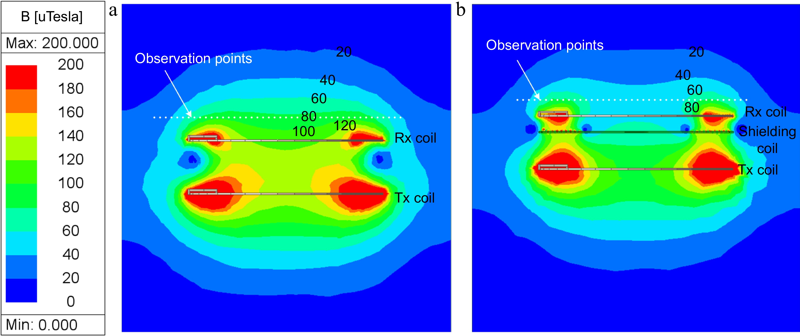
Figure 11.
Distribution of the simulated magnetic field: (a) without, (b) with the resonant reactive shield.
-
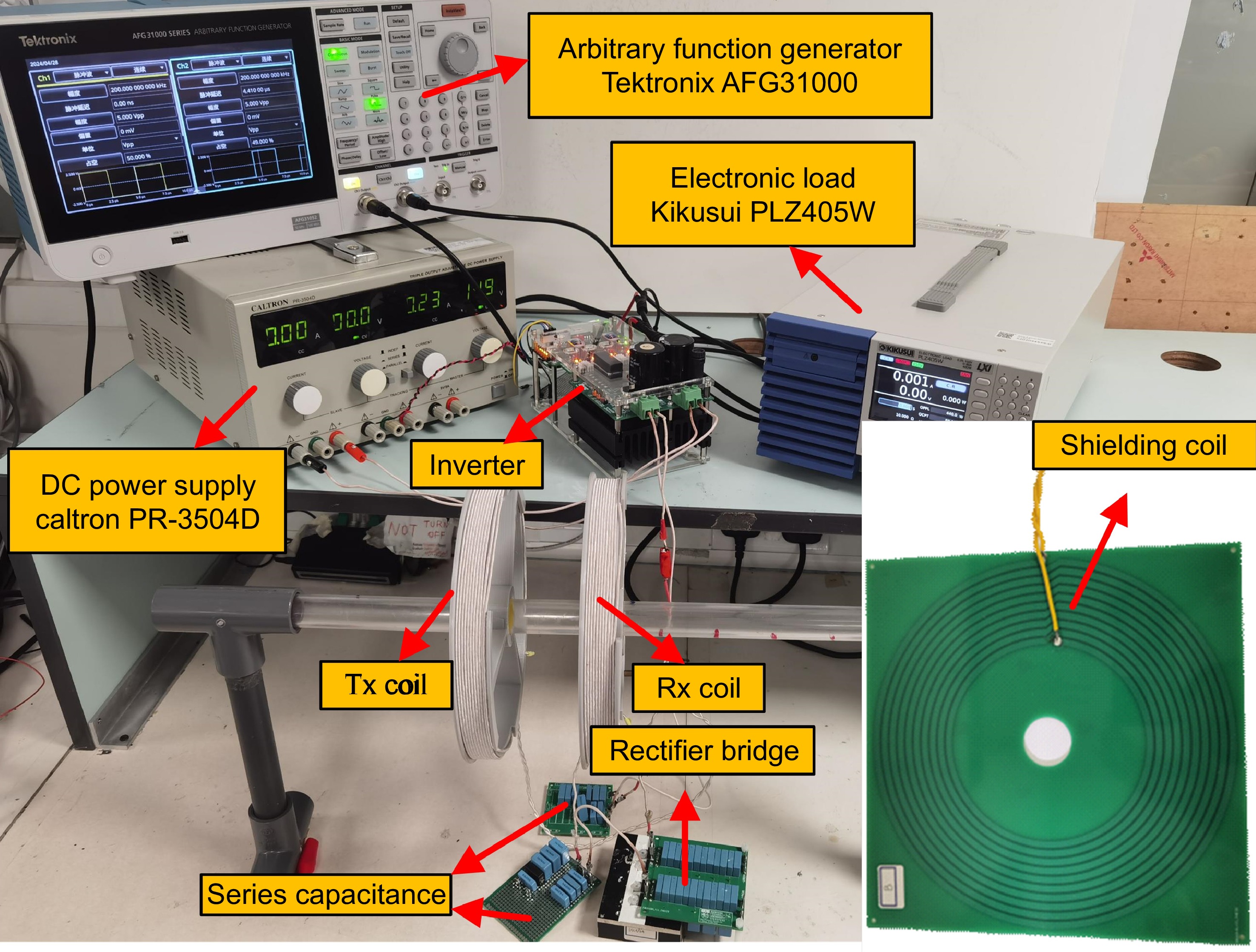
Figure 12.
Photograph of the experiment setup.
-
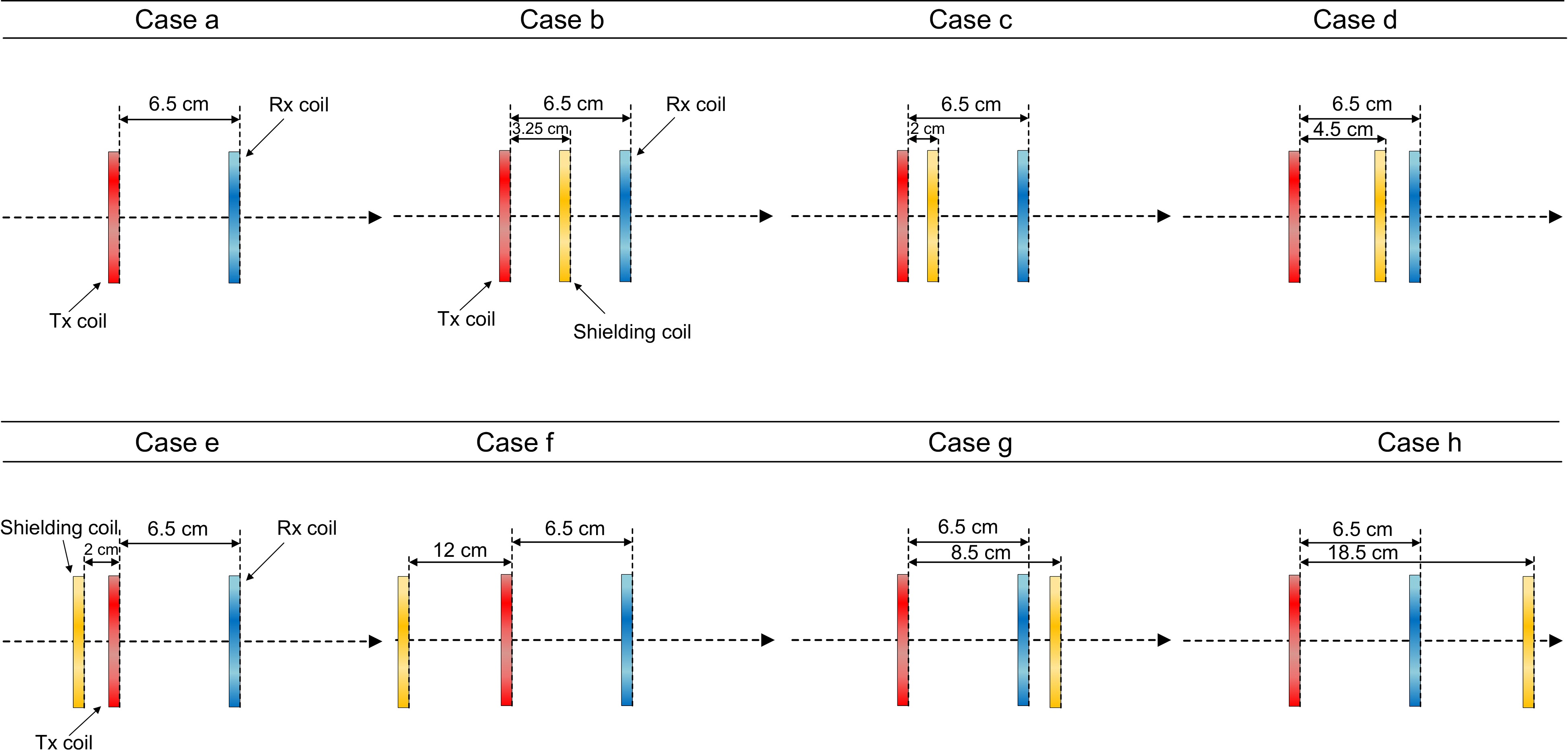
Figure 13.
Schematic diagram of shielding coil placed in different positions (parallel to the transmitting coil).
-
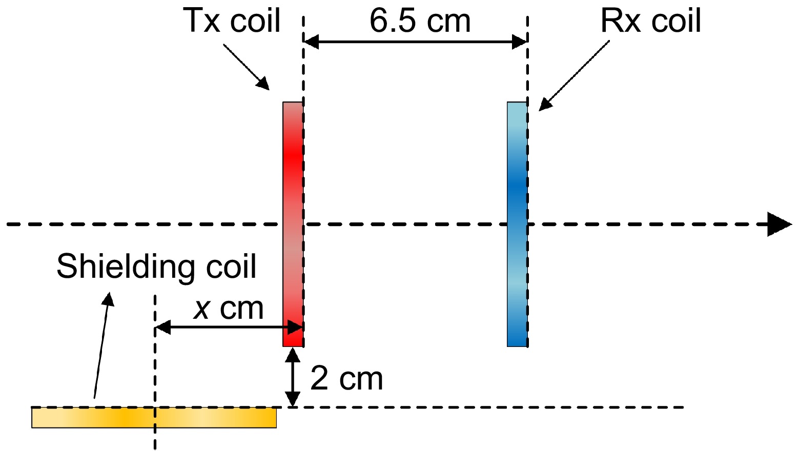
Figure 14.
Schematic diagram of the shielding coil (perpendicular to the transmitting coil).
-
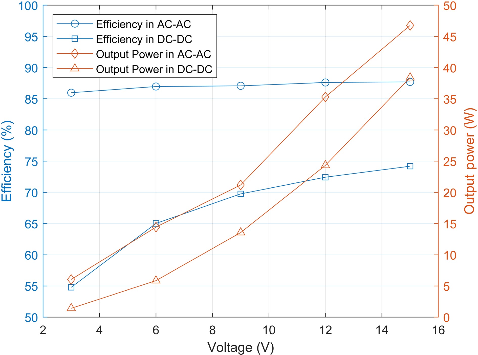
Figure 15.
Efficiency between resonator or WPT system and output power of Rx coil or rectifier bridge in Experiment A.
-

Figure 16.
(a) Efficiencies, and (b) output powers of the WPT system in Experiment A from Case a to h.
-
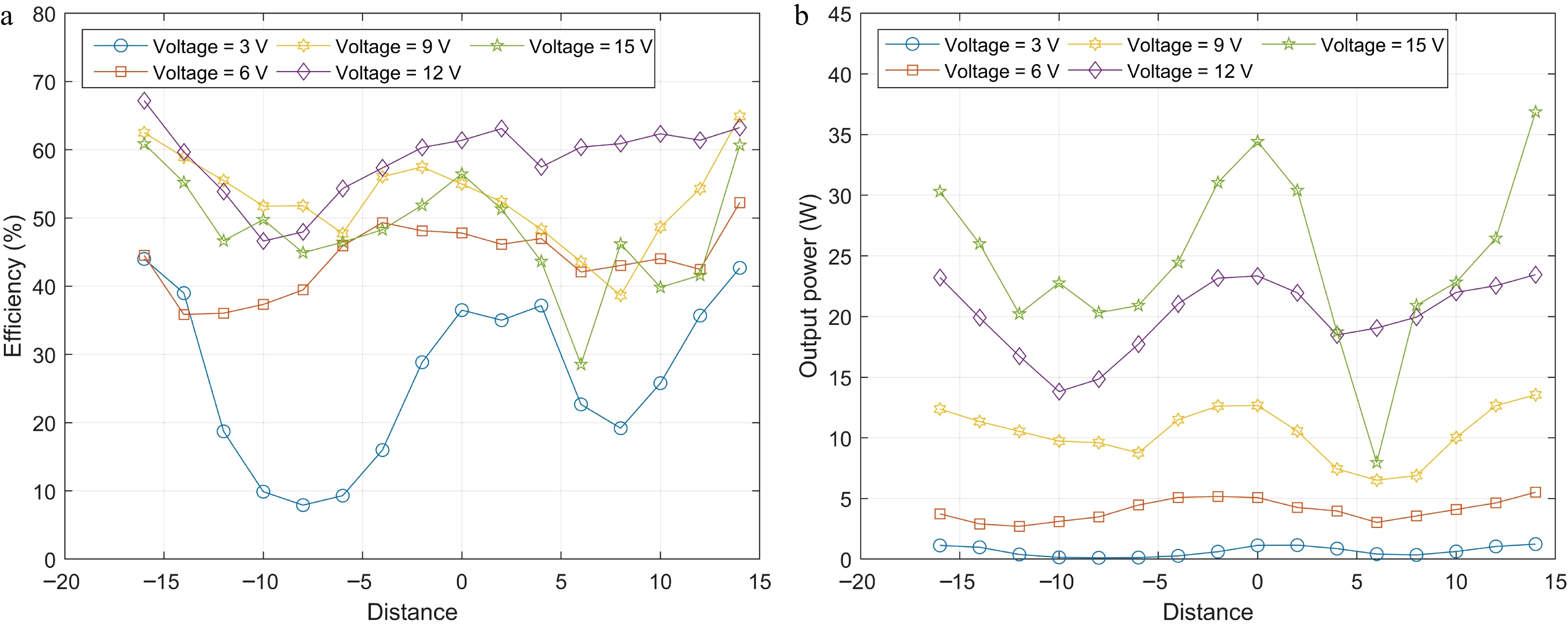
Figure 17.
(a) Efficiencies, and (b) output powers of the WPT system at different voltages in Experiment A when the shielding coil is perpendicular to the transmitting coil.
-
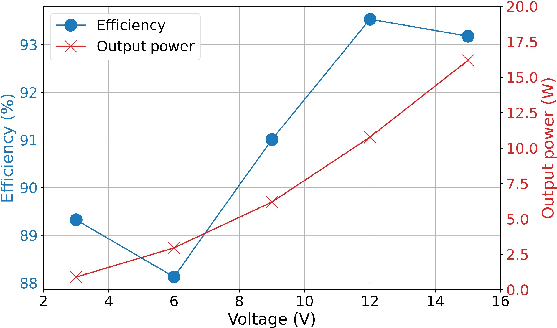
Figure 18.
Efficiency between resonator or WPT system and output power of Rx coil or rectifier bridge in Experiment B.
-

Figure 19.
(a) Efficiencies, and (b) output powers of the WPT system in Experiment B from Case a to h.
-
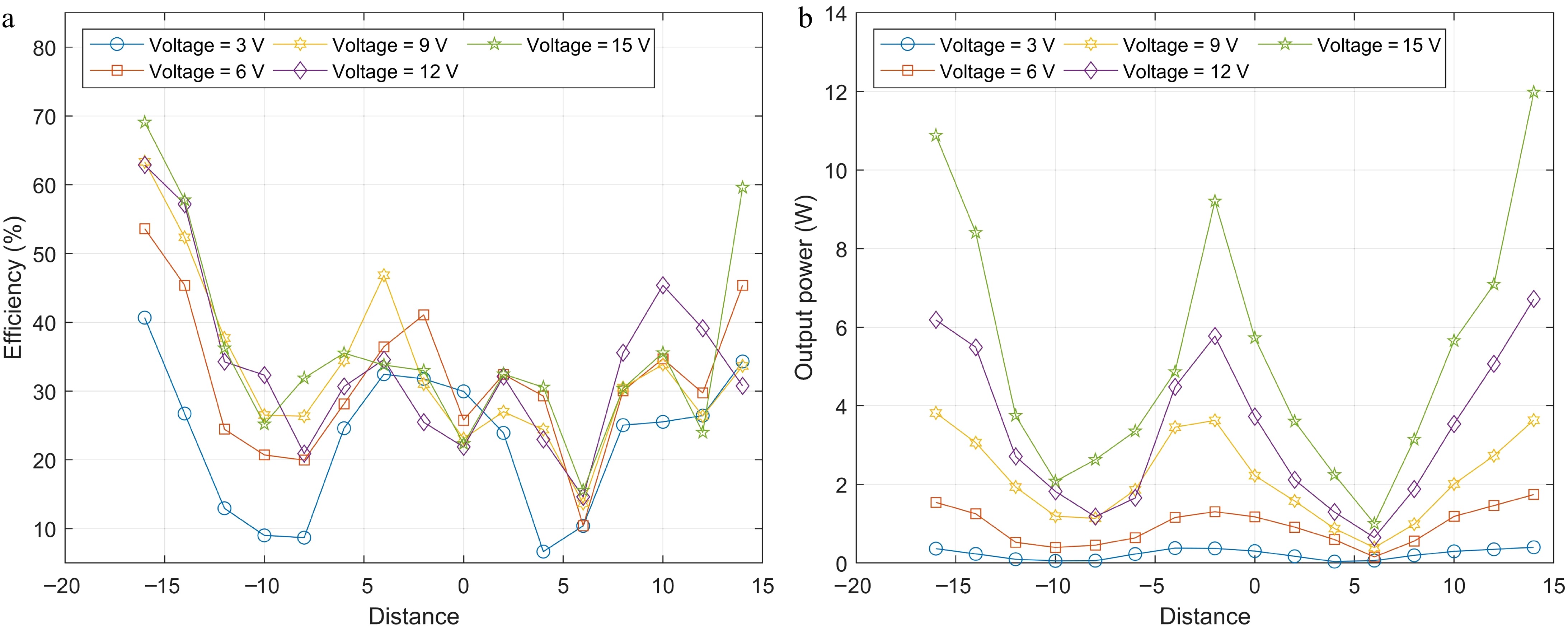
Figure 20.
(a) Efficiencies, and (b) output powers of the WPT system at different voltages in Experiment B when the shielding coil is perpendicular to the transmitting coil.
-
Parameters Value Number of turns 9 Outermost turn width 3.71 mm Outermost radius 113.54 mm Ratio between adjacent turns 0.999 Ratio of central hole 15 mm Space between adjacent turns 1.75 mm Thickness of copper 0.035 mm Size of PCB subplate 118 mm × 118 mm × 1.6 mm Opening angle of each turn 5° Table 1.
Parameters of the shielding coil.
-
Parameters Value Load RL 10 Ω Quality factor of transmitter Q1 200 Inductance L2 50 μH -
Parameters Value Operation frequency of Experiment A 100 kHz Operation frequency of Experiment A 200 kHz Number of turns of Tx and Rx coils 11 Radius of Tx coil and Rx coil 10 cm Load 10 Ω Inductance of Tx coil 47.52 μH Inductance of Rx coil 47.75 μH Series capacitance of Tx coil in Experiment A 53.30 nF Series capacitance of Rx coil in Experiment A 53.05 nF Series capacitance of Tx coil in Experiment B 13.33 nF Series capacitance of Rx coil in Experiment B 13.26 nF Distance between Tx coil and Rx coil 6.5 cm Mutual induction of Tx coil and Rx coil 9.847 μH Wire diameter of Tx coil and Rx coil 1.8 mm Table 3.
Parameters for WPT system used in the experiments.
Figures
(20)
Tables
(3)