-

Figure 1.
Overall circuit structure of the proposed WPT system and circuit structure of the WPT system working in CV mode.
-
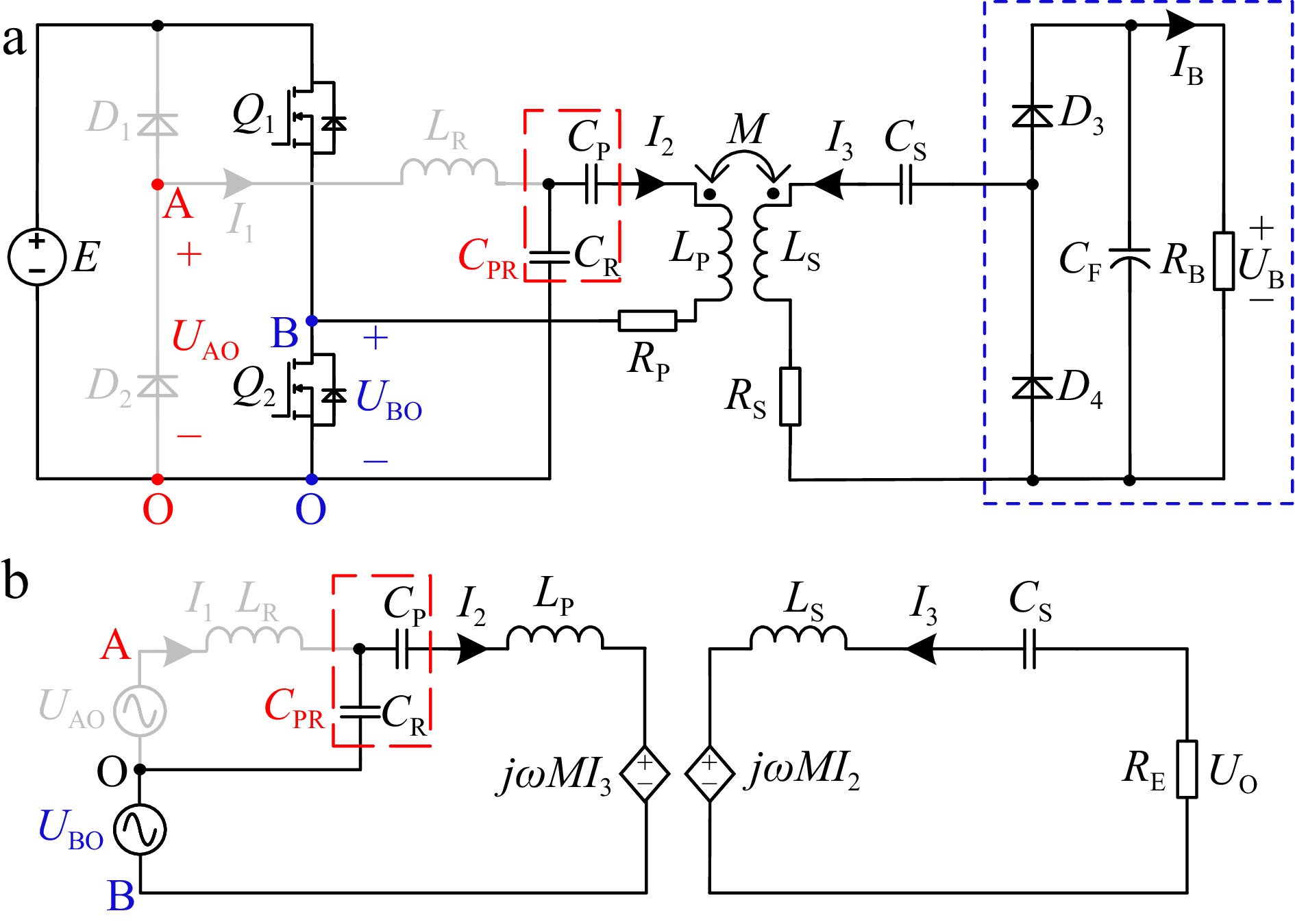
Figure 2.
Circuit structure and equivalent circuit of the WPT system working in CC mode. (a) Circuit structure diagram. (b) Equivalent circuit diagram.
-
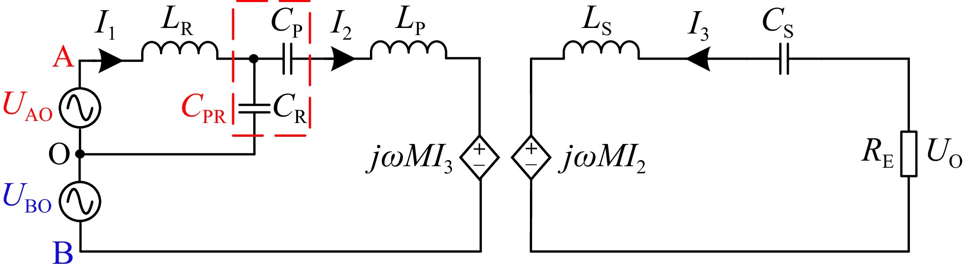
Figure 3.
Equivalent circuit of the WPT system working in CV mode.
-
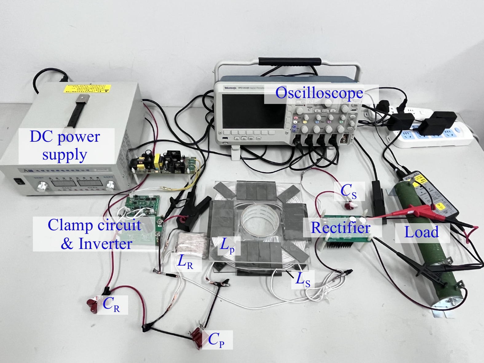
Figure 4.
Experimental prototype.
-

Figure 5.
Experimental waveforms. (a) RB = 5 Ω. (b) RB = 10 Ω. (c) RB = 30 Ω. (d) RB = 40 Ω. (e) RB = 100 Ω. (f) RB = 150 Ω.
-
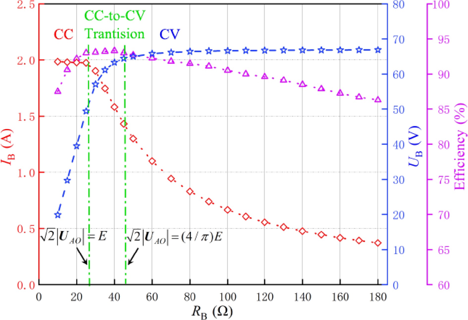
Figure 6.
Measured IB, UB, and efficiency curve vs RB.
-
Parameters Value CP, CS, CR (nF) 175.4, 175.4, 175.4 LP, LS, LR, M (μH) 50, 50, 28.5, 19.2 Table 1.
Specific compensation parameters of the proposed system.
Figures
(6)
Tables
(1)