-
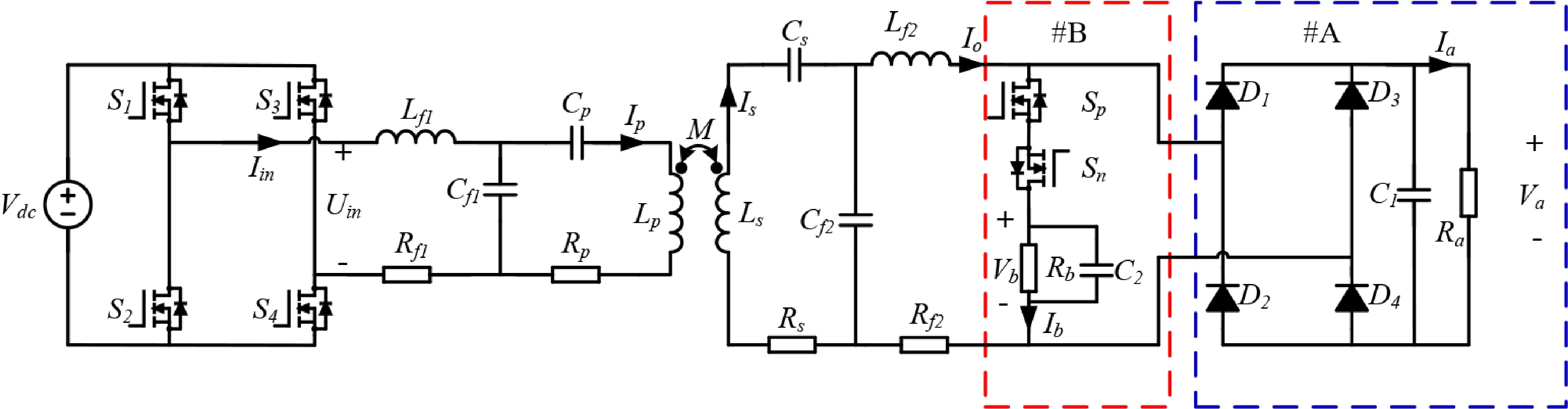
Figure 1.
Topology of the dual-load WPT system with constant-voltage and constant-current capabilities.
-
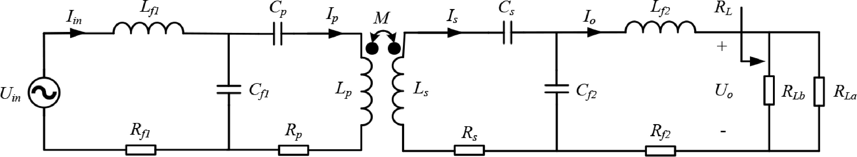
Figure 2.
Equivalent circuit model.
-
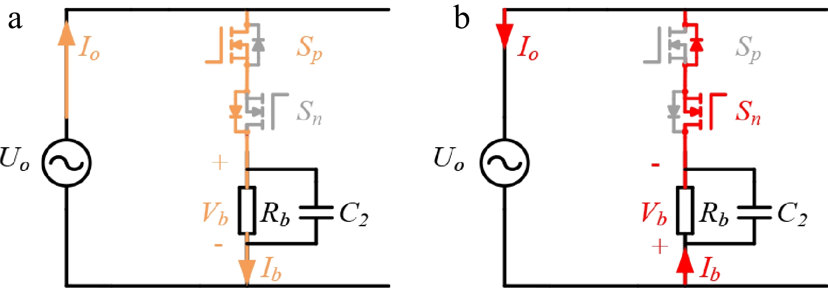
Figure 3.
Equivalent circuit of #B output circuit. (a) Forward conduction mode. (b) Reverse conduction mode.
-
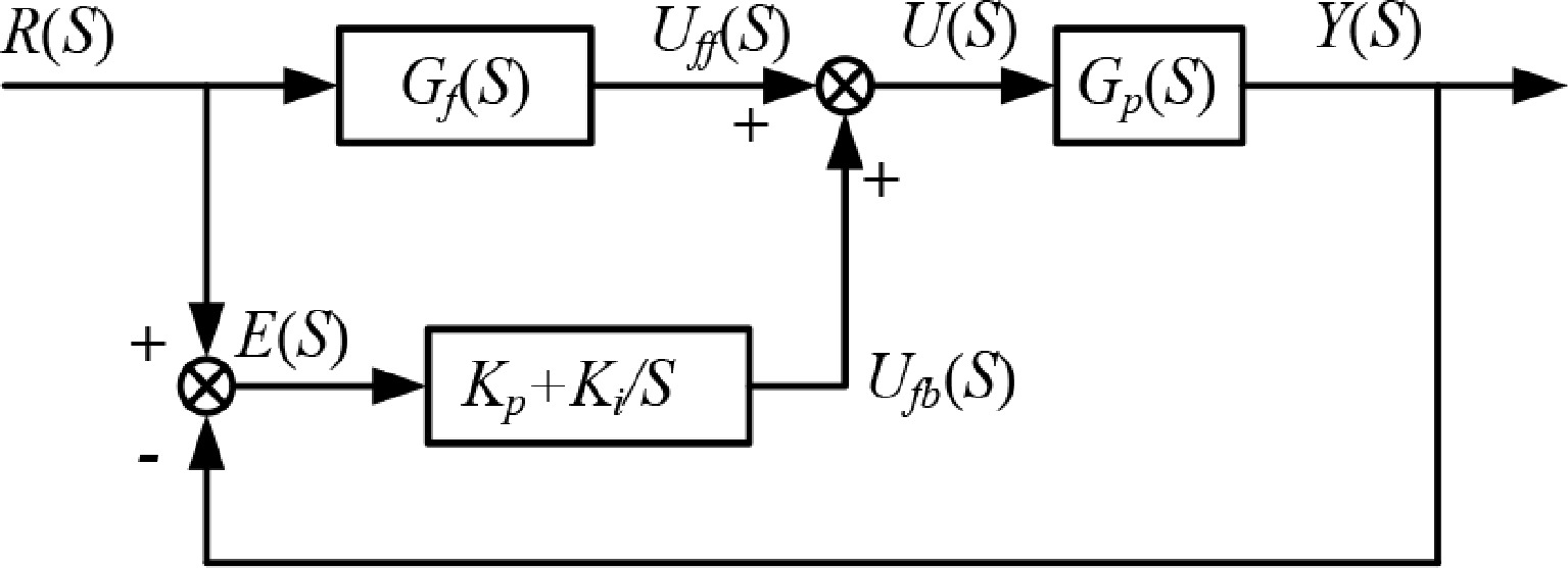
Figure 4.
Schematic diagram of feedforward PI control.
-
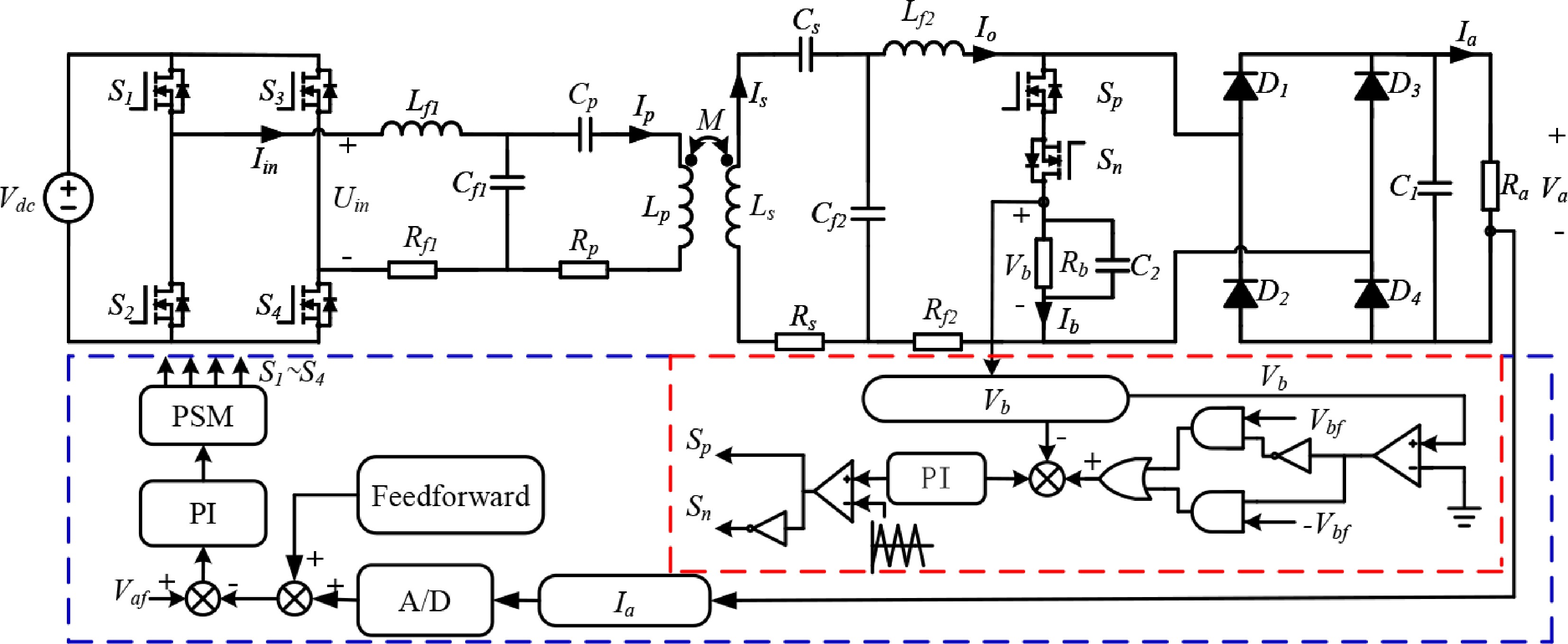
Figure 5.
Schematic diagram of the composite control strategy for dual-load WPT systems.
-
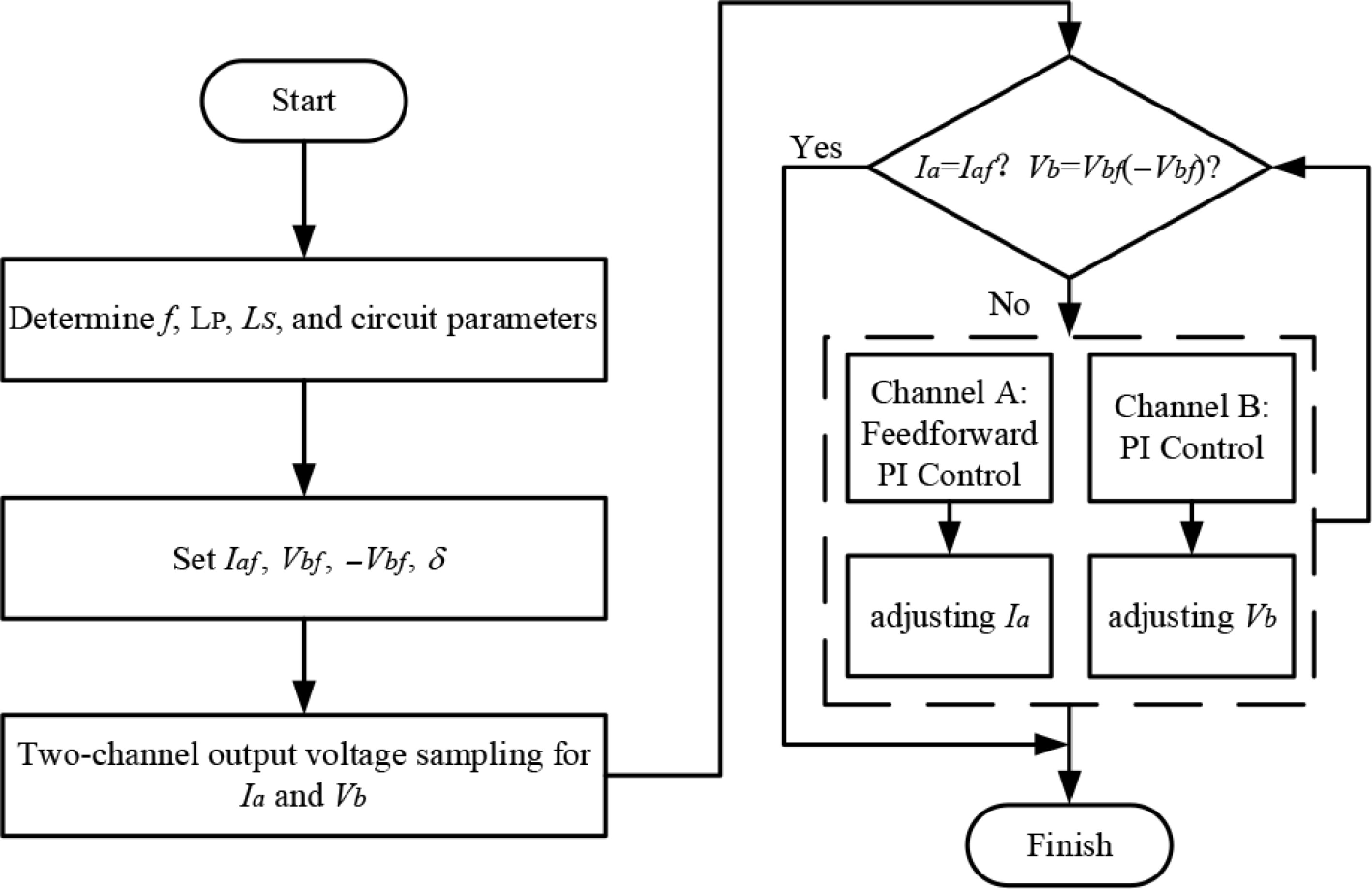
Figure 6.
System operation flowchart.
-
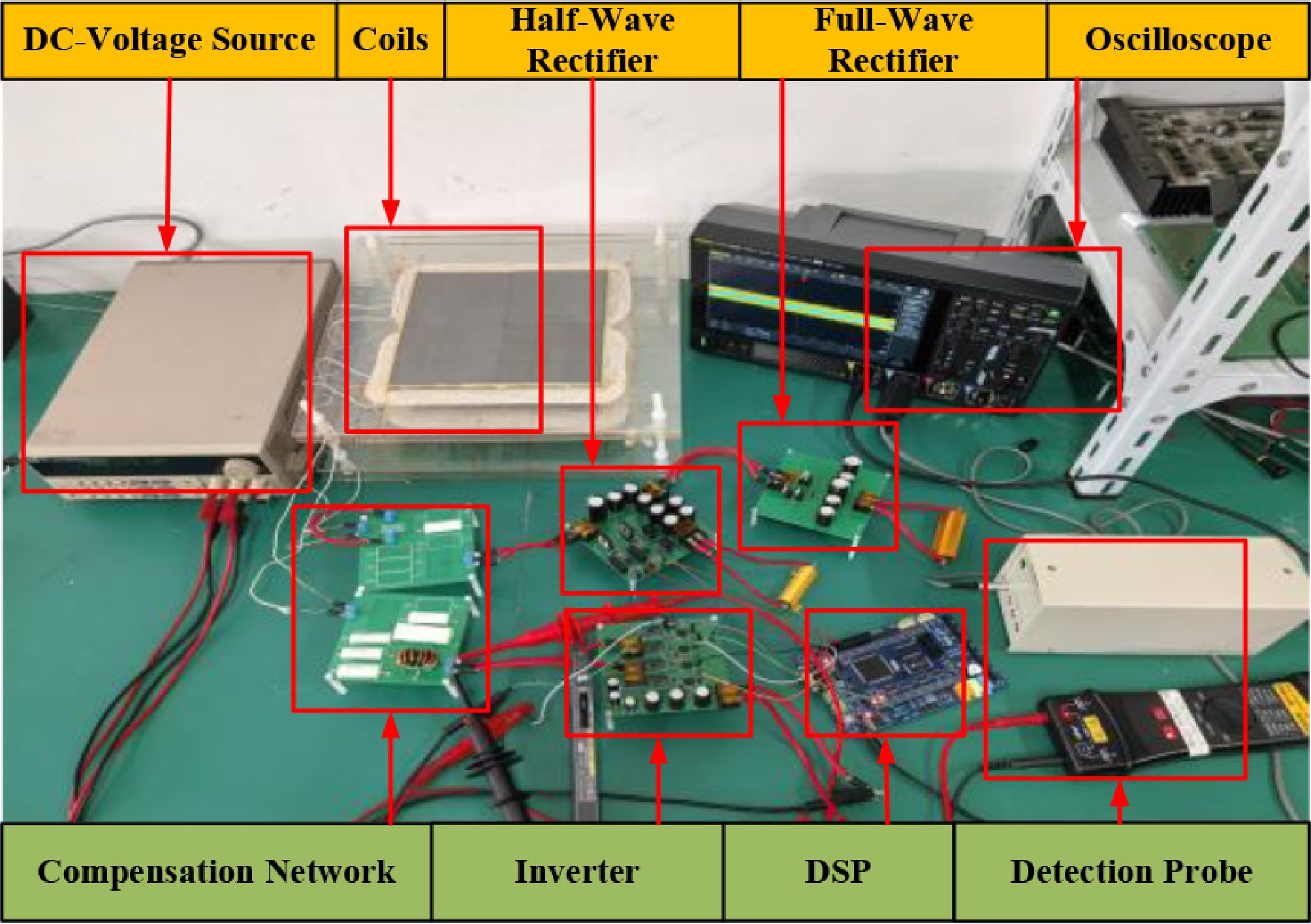
Figure 7.
Experimental platform.
-
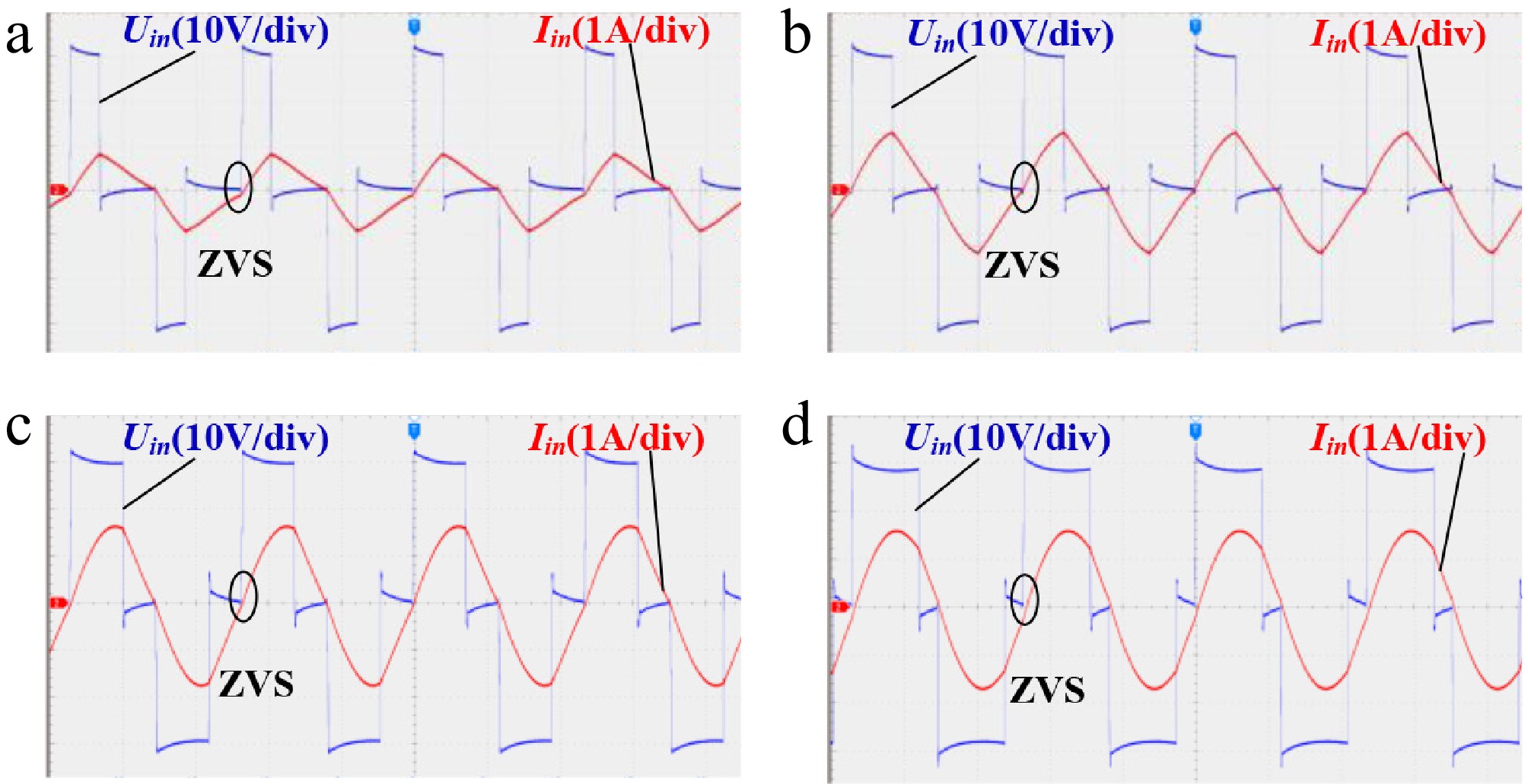
Figure 8.
Waveforms of the inverter's output voltage and current under different reference values. (a) Ia = 1 A,Vb = ±5 V. (b) Ia = 1.2 A,Vb = ±10 V. (c) Ia = 2 A,Vb = ±15 V. (d) Ia = 2.4 A,Vb = ±25 V.
-
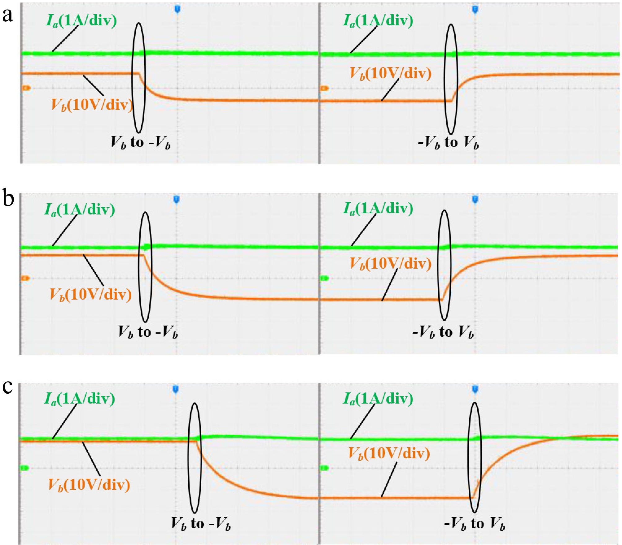
Figure 9.
Verification waveforms of independent power regulation. (a) Ia = 1.6 A,Vb = ±7.5 V. (b) Ia = 1.6 A, Vb = ±10 V. (c) Ia = 1.6 A,Vb = ±15 V.
-
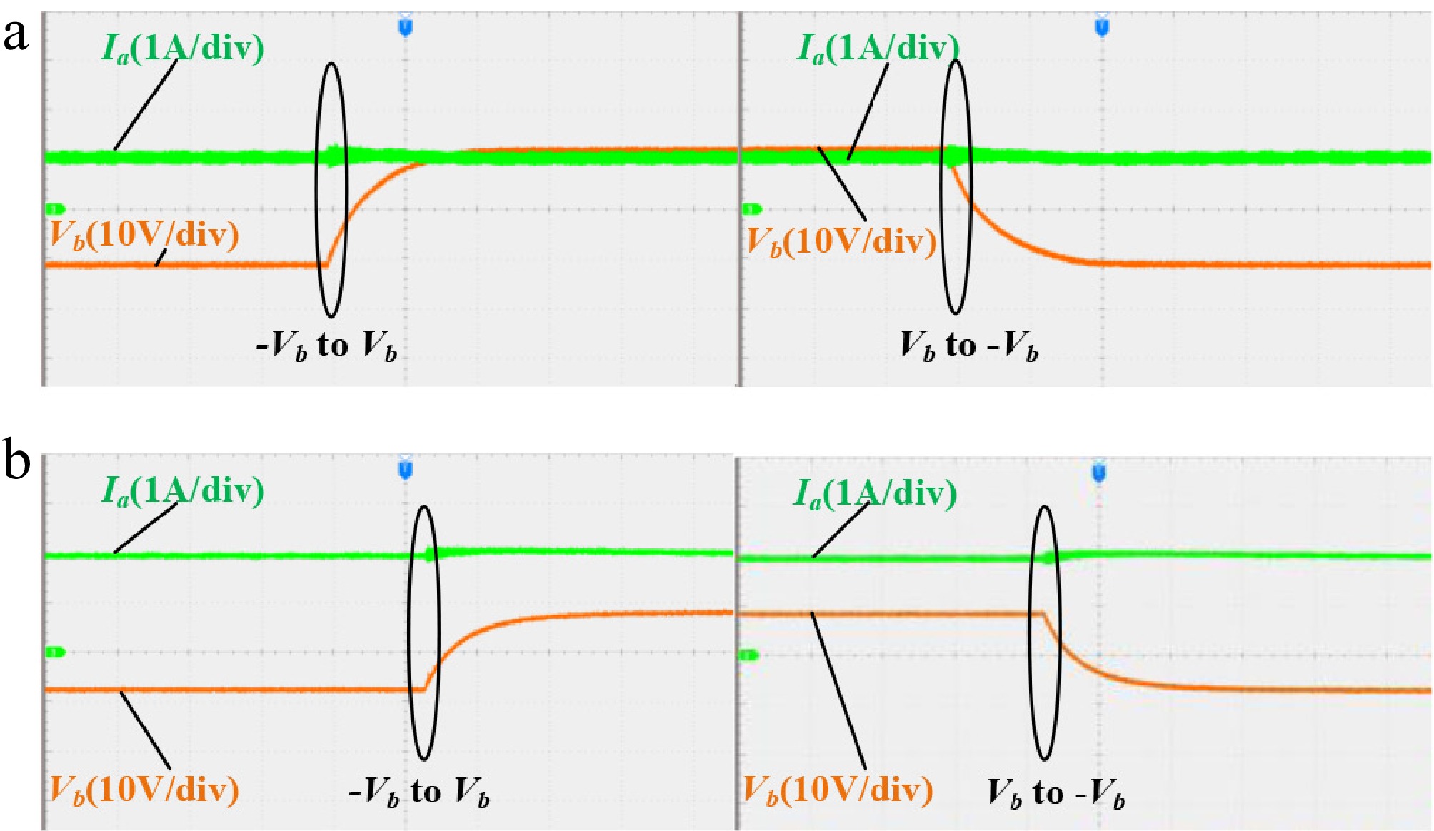
Figure 10.
Experimental waveforms of Vb polarity switching. (a) Ia = 1.2 A,Vb = ±10 V. (b) Ia = 2 A,Vb = ±10 V.
-
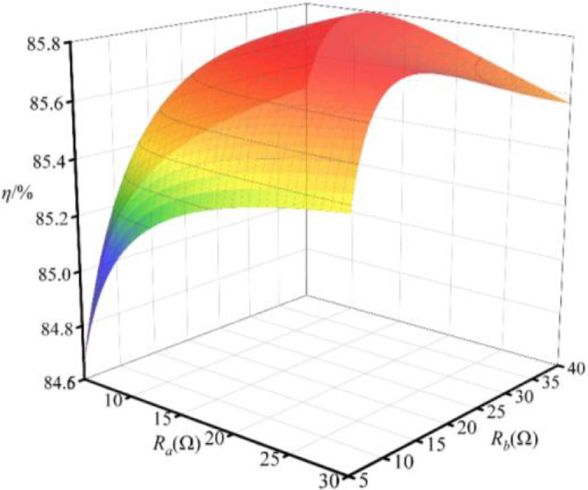
Figure 11.
System transmission efficiency.
-
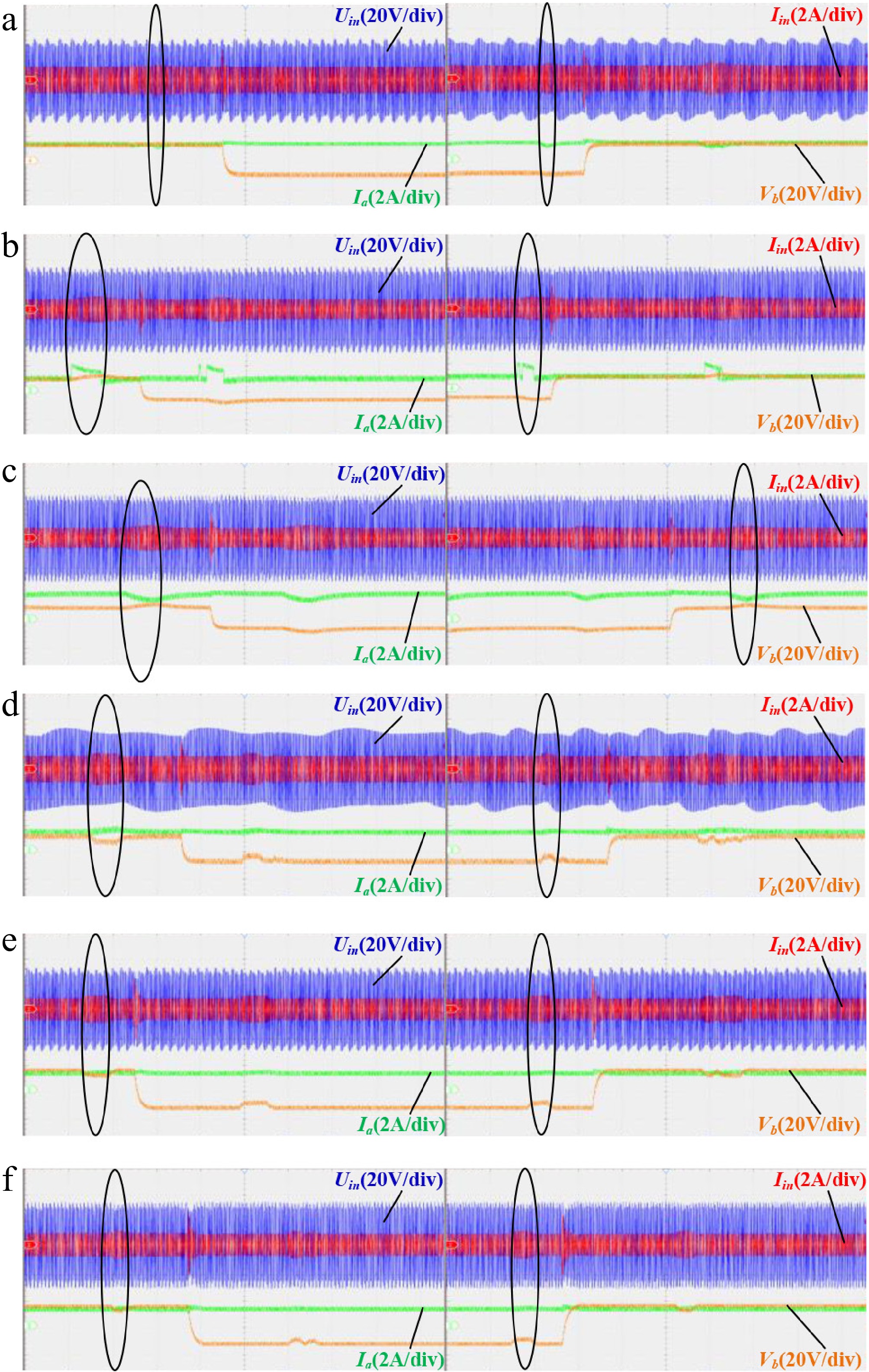
Figure 12.
Dynamic response of the system. (a) Ra: 10 Ω→5 Ω→10 Ω. (b) Ra: 10 Ω→20 Ω→10 Ω. (c) Ra: 20 Ω→10 Ω→20 Ω. (d) Rb: 10 Ω→5 Ω→10 Ω. (e) Rb: 10 Ω→20 Ω→10 Ω. (f) Rb: 20 Ω→10 Ω→20 Ω.
-
Item Value Item Value Vdc 30 V f 85 KHz LP 247.40 μH CP 16.16 nF LS 110.69 μH CS 45.13 nF Lf1 30 μH Cf1 116.86 nF Lf2 33 μH Cf2 106.24 nF RP 0.2 Ω Rf1 0.07 Ω RS 0.14 Ω Rf2 0.09 Ω Table 1.
Experimental parameters.
Figures
(12)
Tables
(1)