-
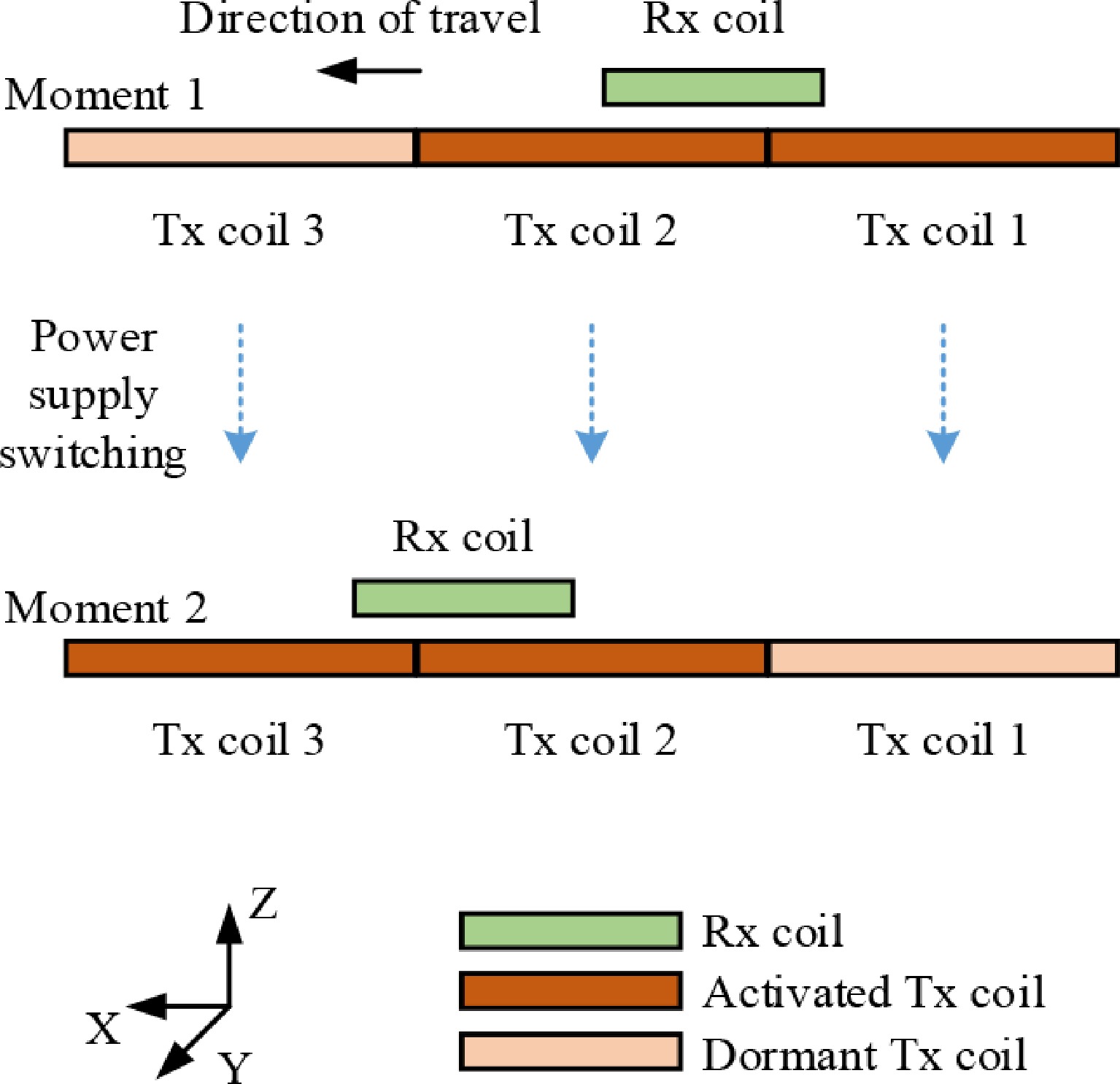
Figure 1.
Power supply timing model for an array-type DWPT system.
-
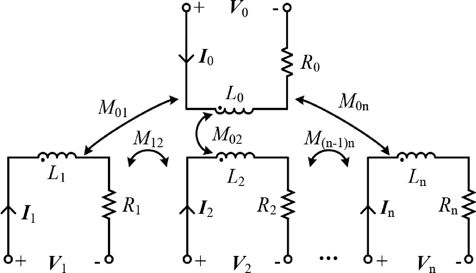
Figure 2.
Typical mutual inductance model of an array-type DWPT system.
-
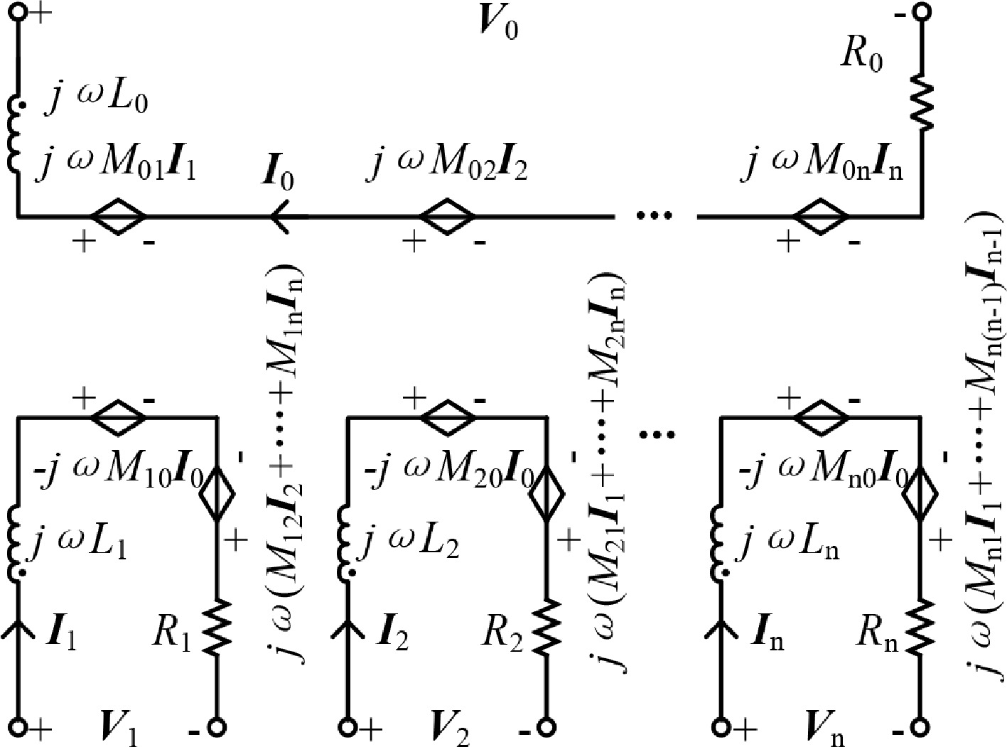
Figure 3.
Controlled source model of an array-type DWPT system.
-
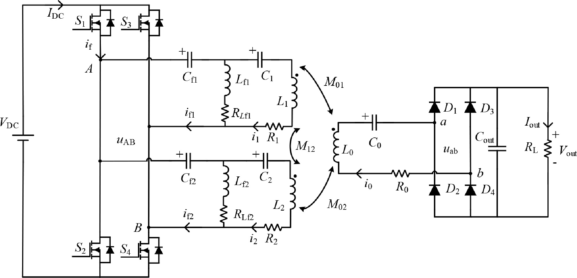
Figure 4.
CLC-S compensated DISO system.
-
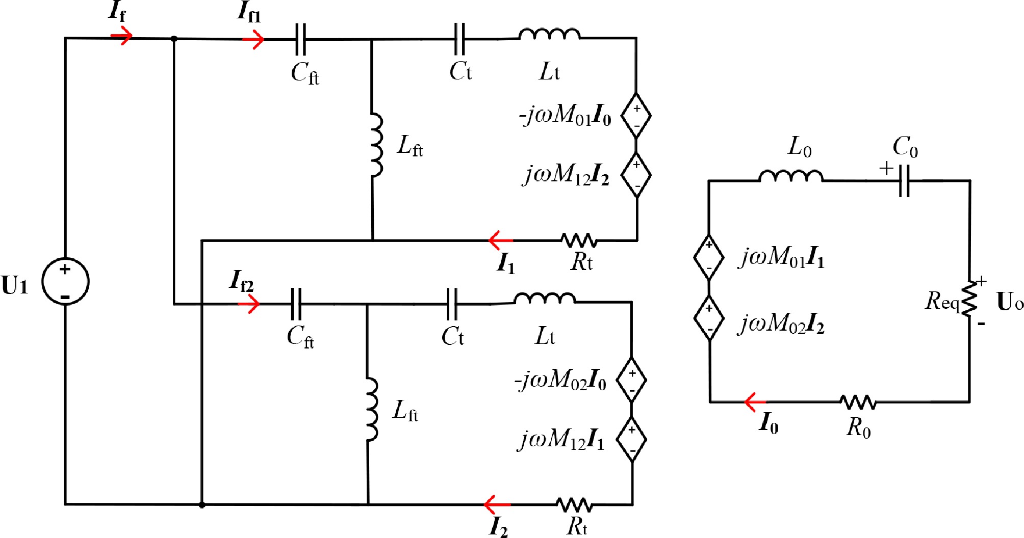
Figure 5.
Simplified equivalent circuit of a CLC-S compensated DISO system.
-
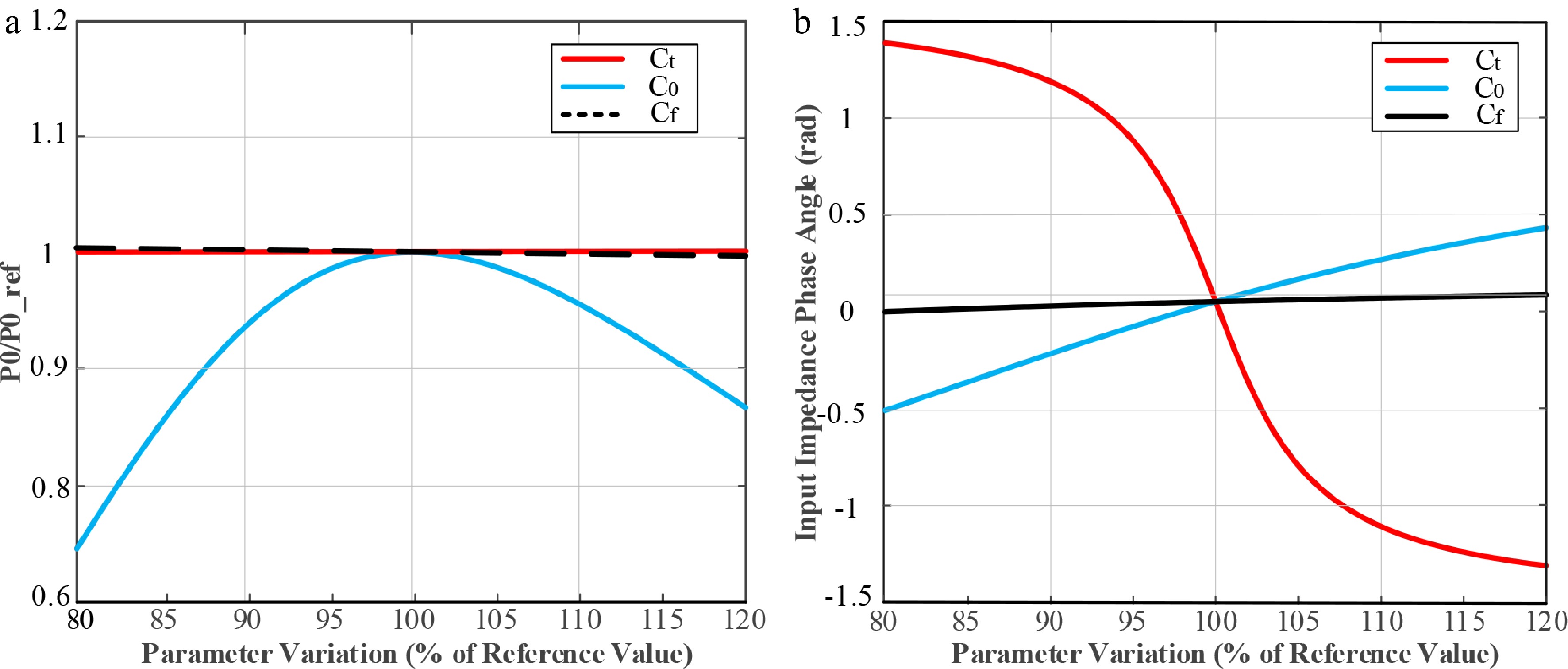
Figure 6.
The transfer characteristics vs compensation capacitance: (a) output power; (b)input impedance phase angle.
-
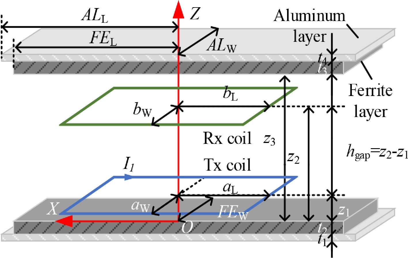
Figure 7.
Schematic diagram of the magnetic coupler.
-
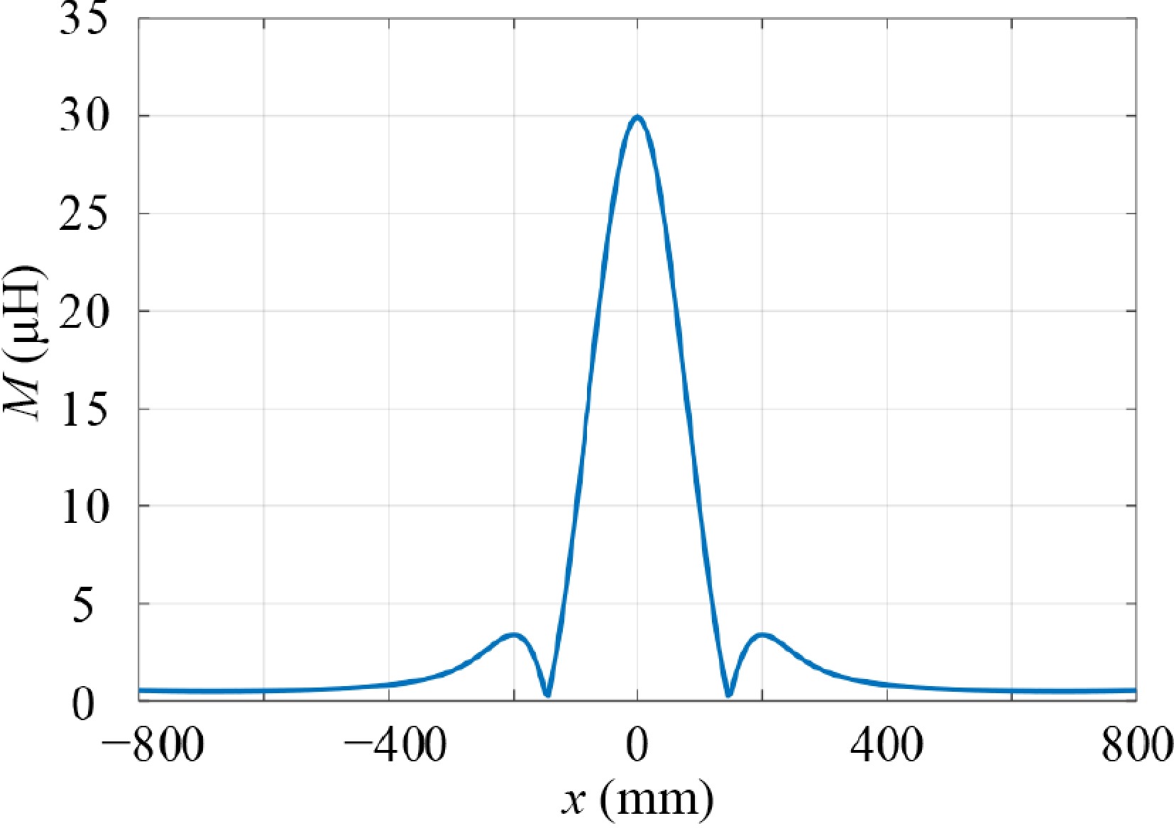
Figure 8.
Characteristic curve of M as a function of the position of the Rx coil.
-
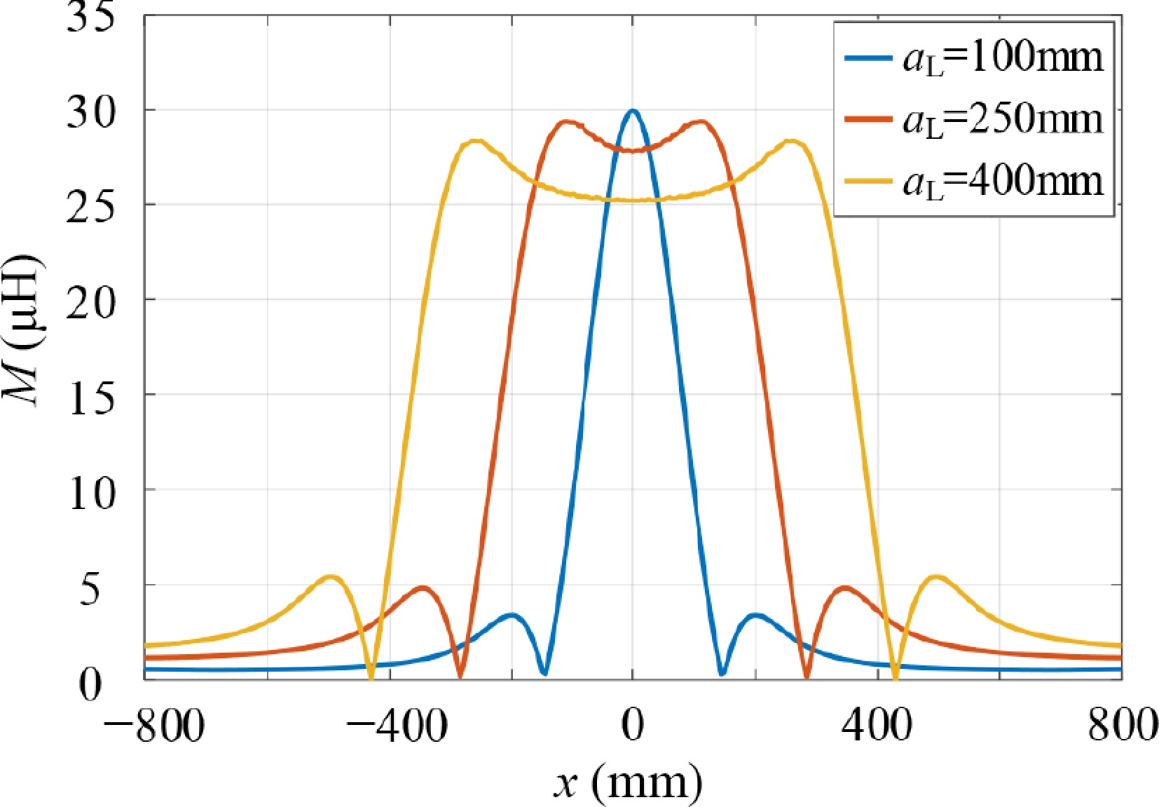
Figure 9.
Change of M as a function of the position of the Rx coil (with different length of the Tx coil in the X direction).
-
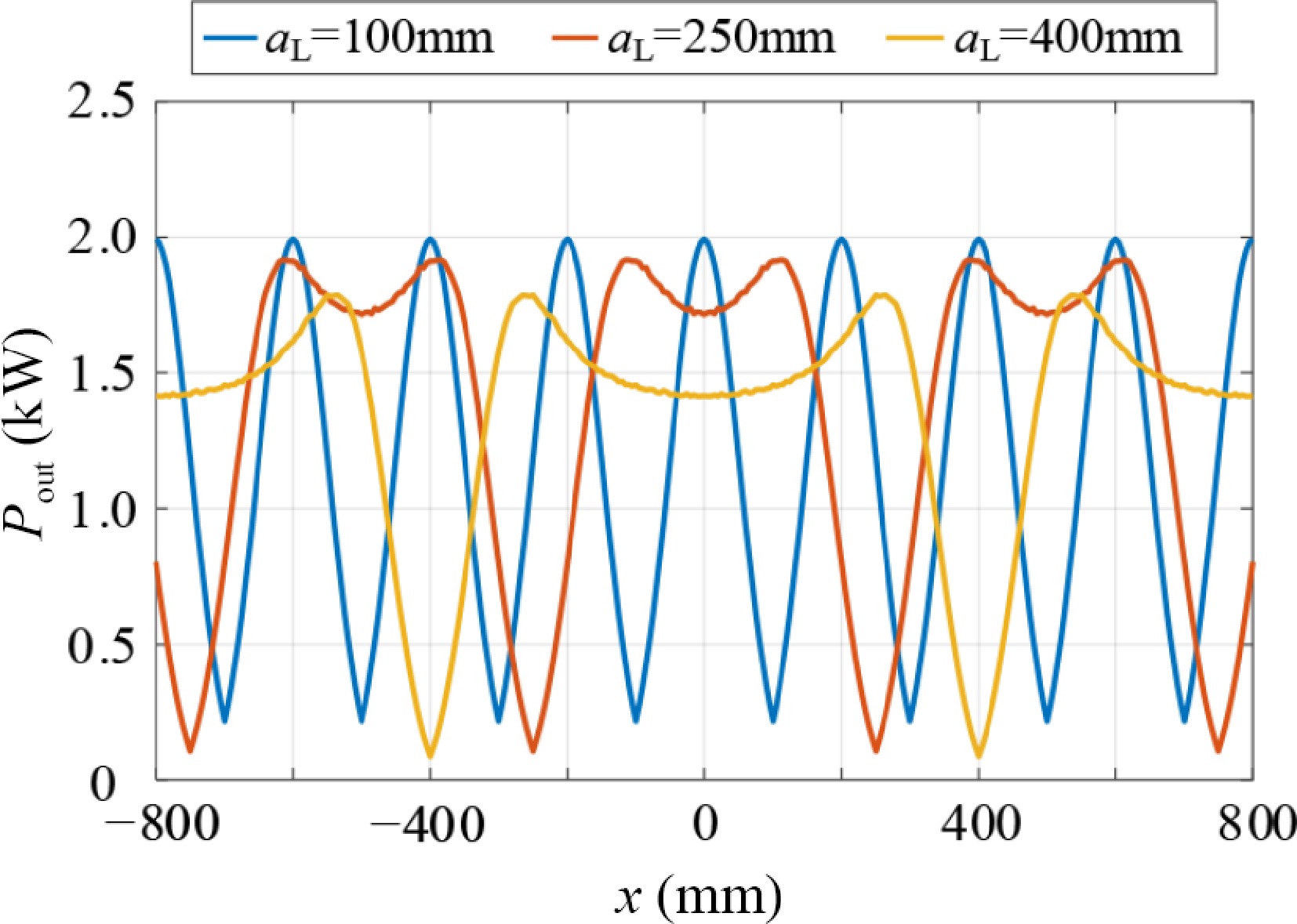
Figure 10.
Fluctuation curve of the output power.
-
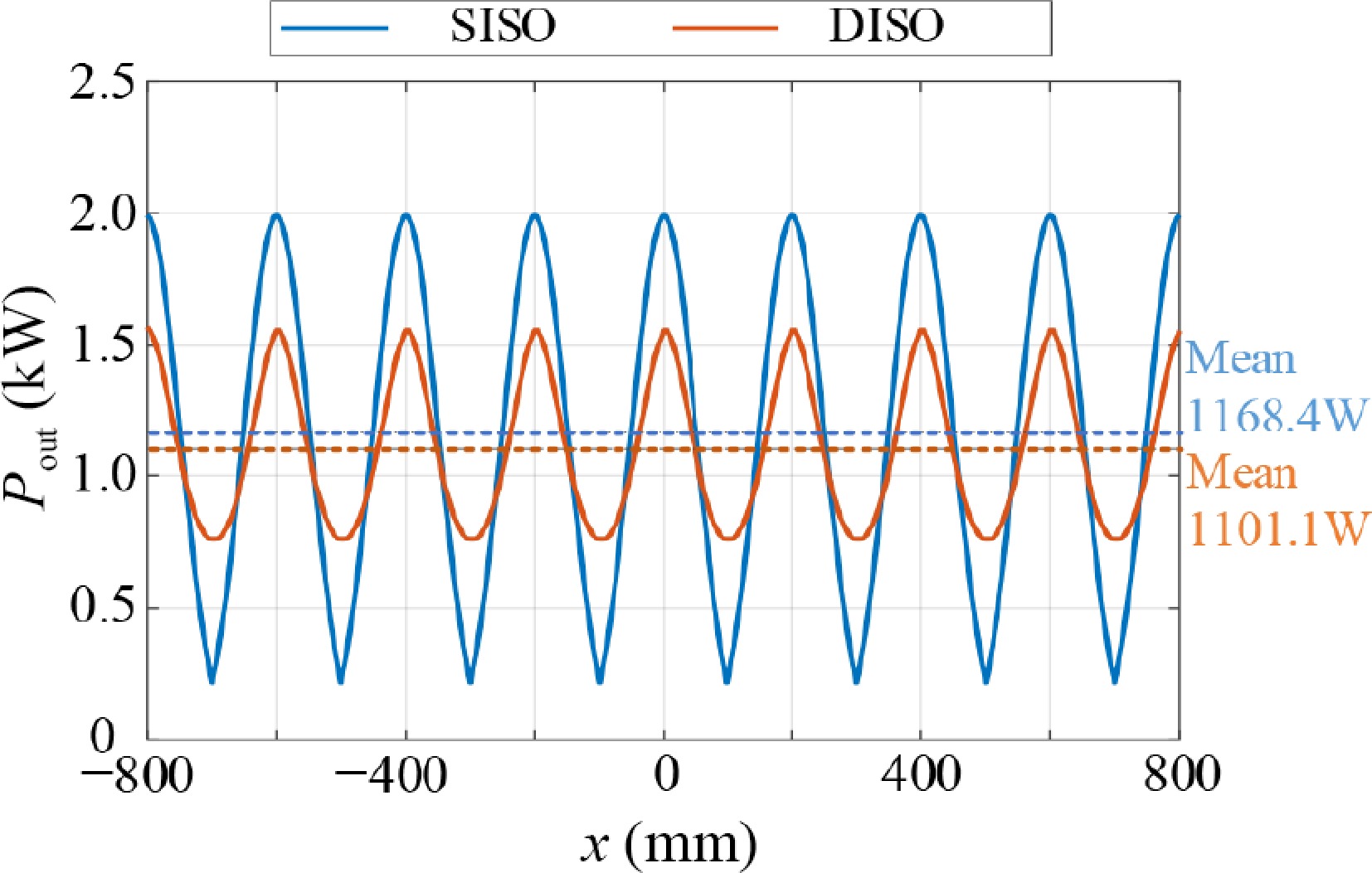
Figure 11.
Fluctuation curve of the output power of the CLC-S compensated SISO and DISO system (
$ {a}_{\mathrm{L}}=100\text{ mm}) $ -
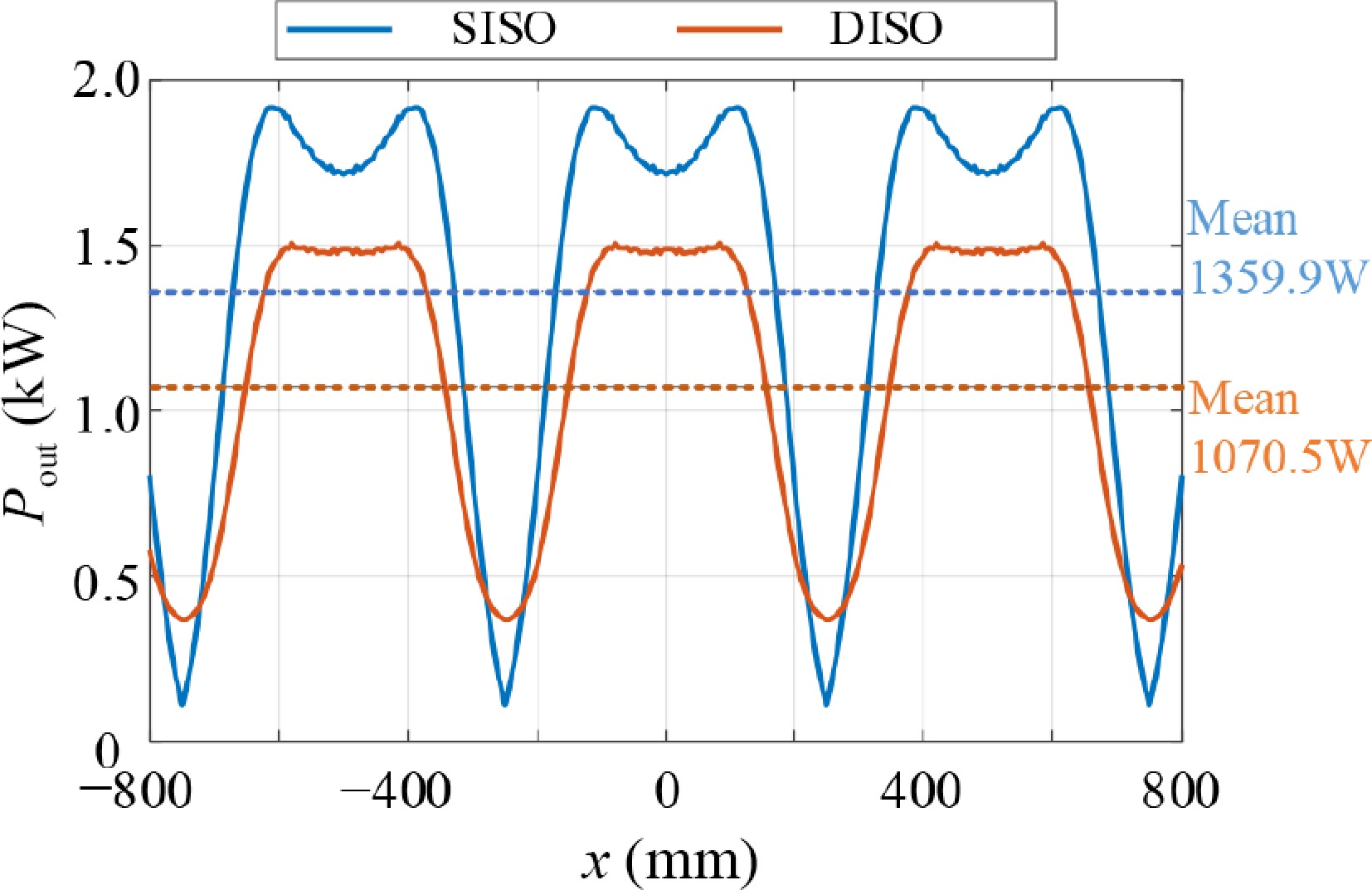
Figure 12.
Fluctuation curve of the output power of the CLC-S compensated SISO and DISO system (aL = 250 mm).
-
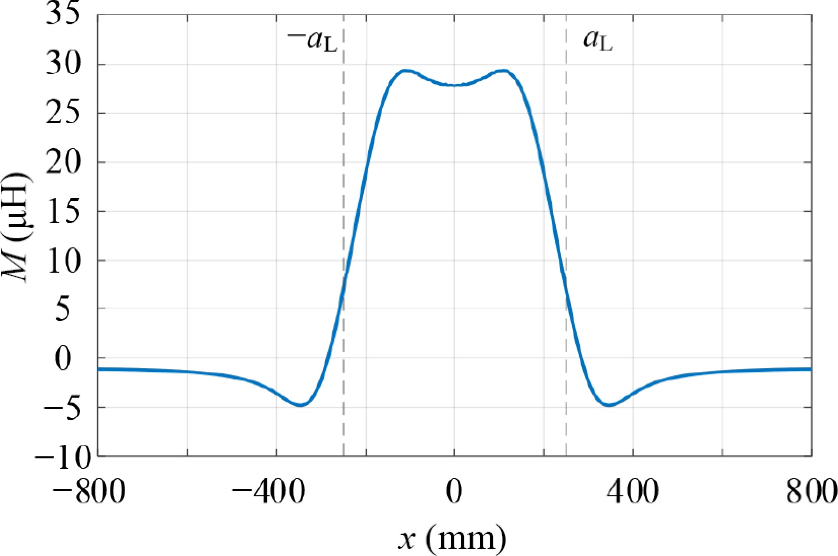
Figure 13.
The mutual inductance value considering the directionality of the magnetic field (aL = 250 mm).
-
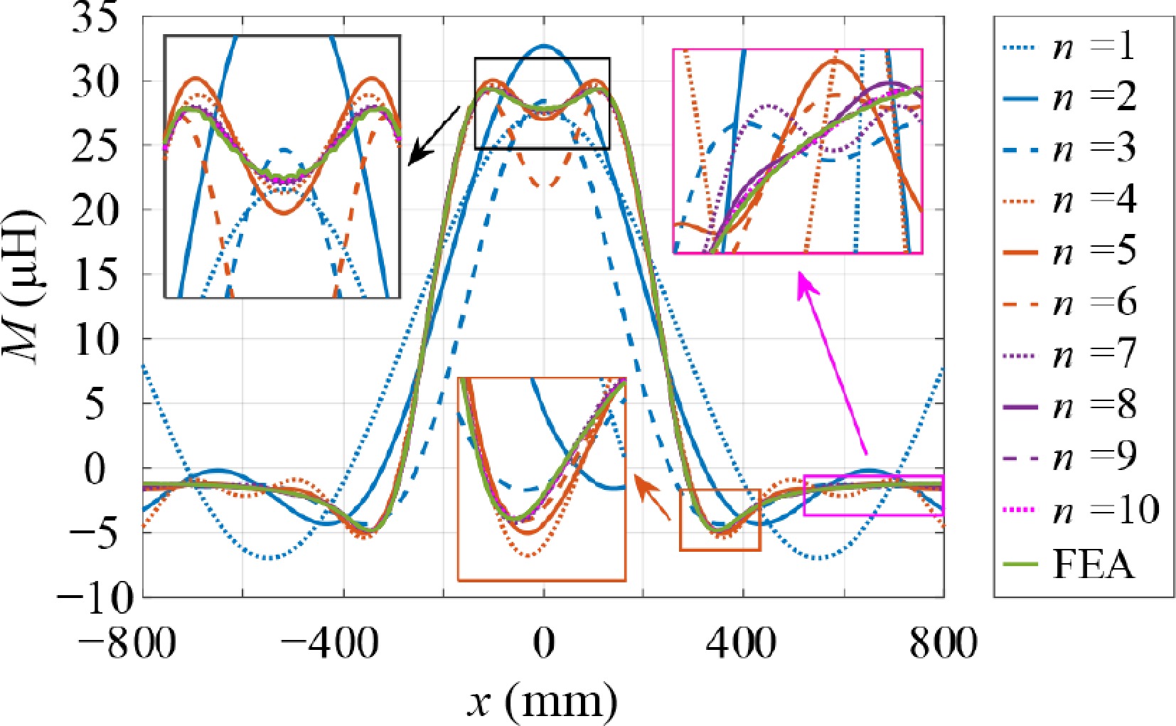
Figure 14.
Fitting situation of Fourier series of different orders.
-
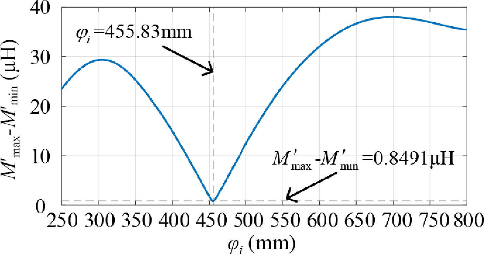
Figure 15.
Fluctuation amplitude of mutual inductance at different
$\varphi _i $ -
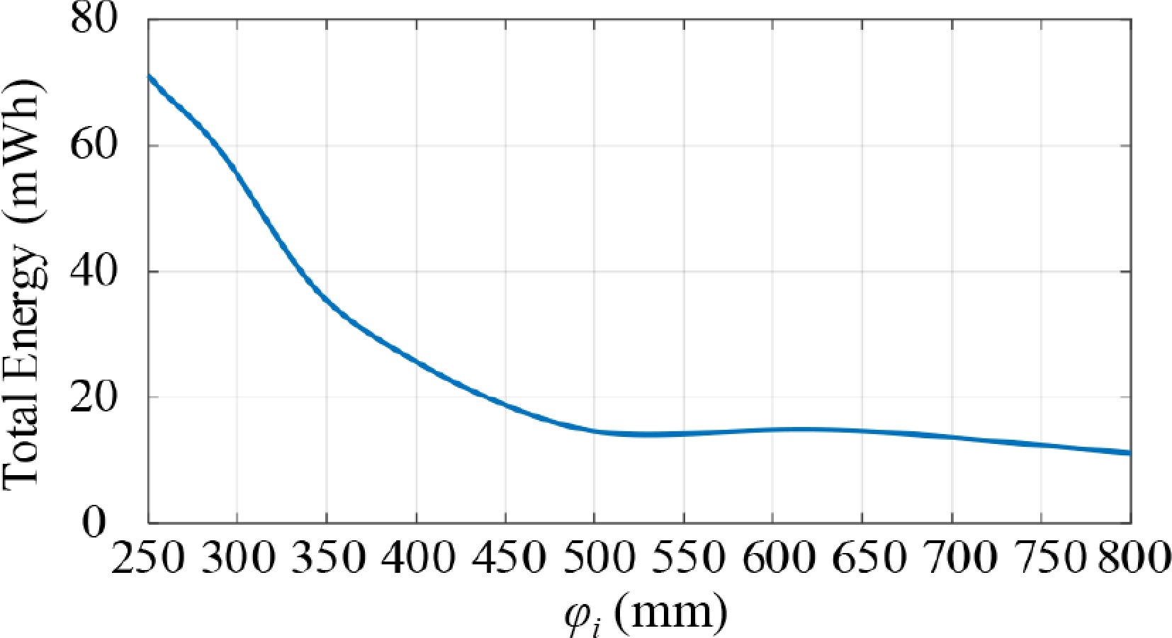
Figure 16.
Total energy transmission curve of the DWPT system under different
$\varphi _i $ -
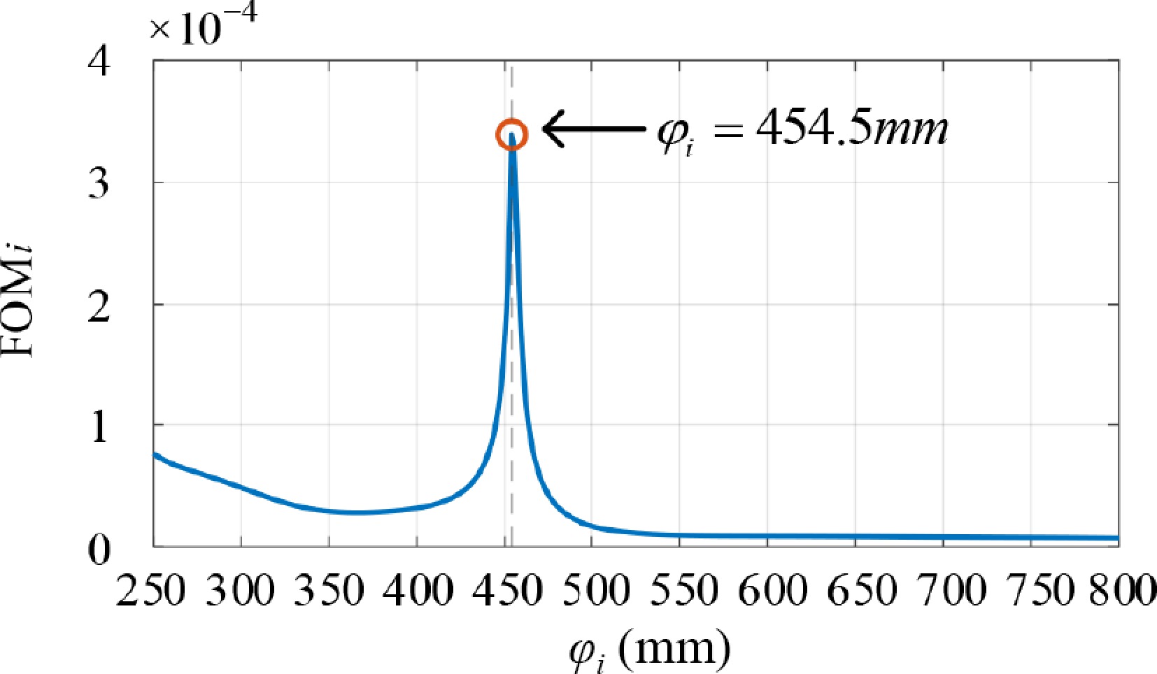
Figure 17.
The curve of FOMi as a function of
$\varphi _i $ -
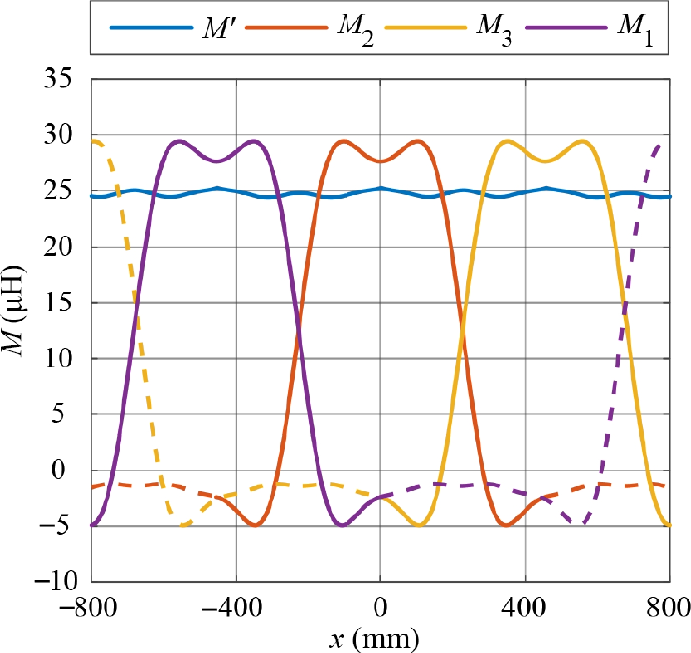
Figure 18.
The mutual inductance fluctuation curve.
-
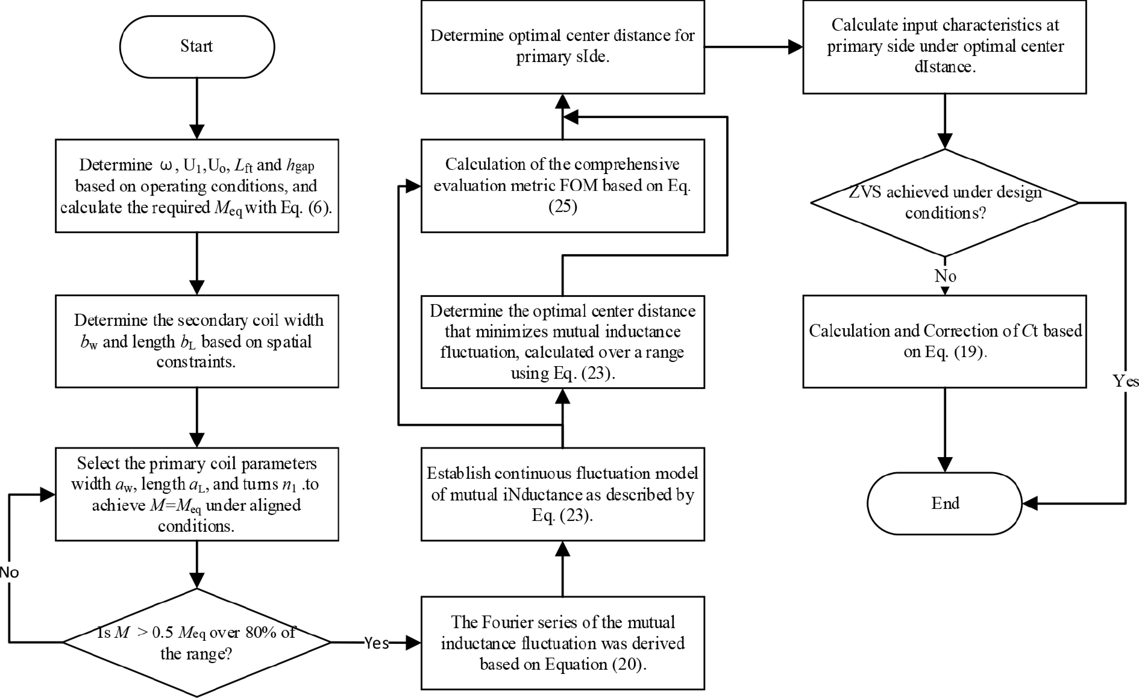
Figure 19.
Design flow of a double-channel WPTS.
-
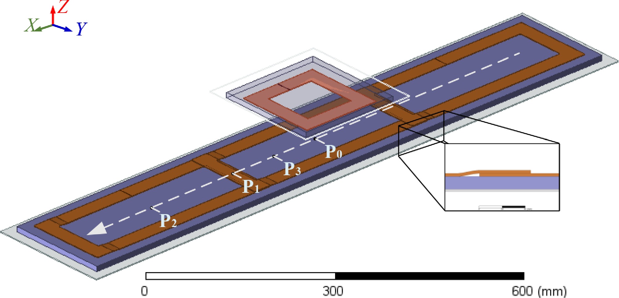
Figure 20.
DISO system magnetic coupler FEA model.
-
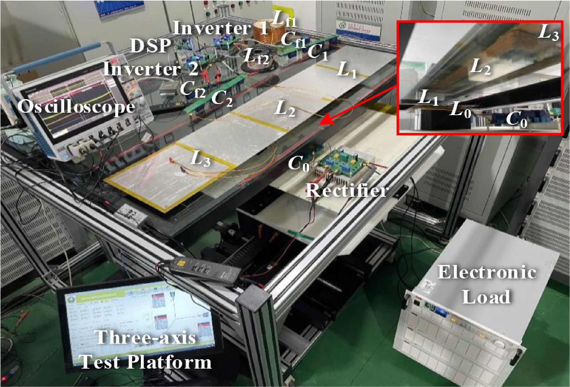
Figure 21.
Laboratory setup of the proposed DWPT system.
-
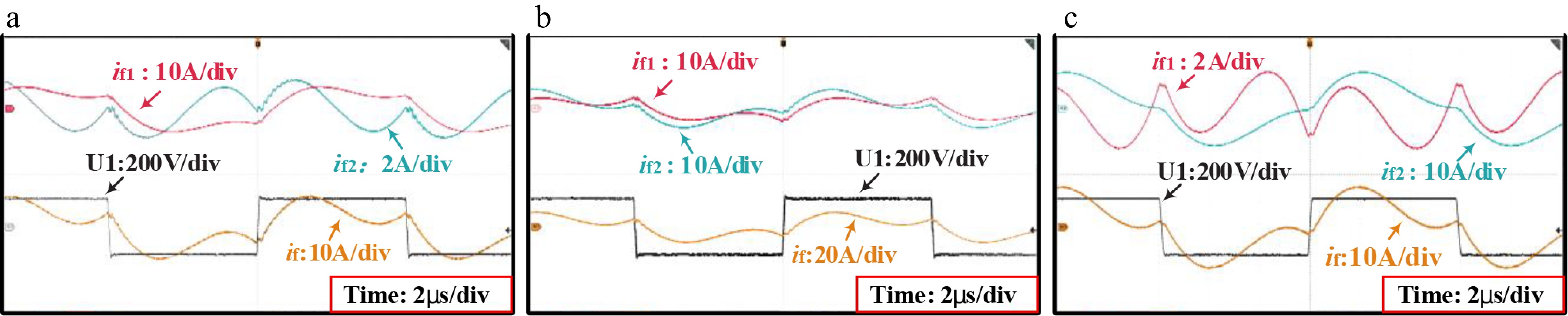
Figure 22.
Current and voltage waveforms at two characteristic positions during dynamic motion. (a) Position P0 (0.0, 1.5), (b) position P1 (227.5, 0, 1.5), (c) position P1 (455, 0, 1.5).
-

Figure 23.
Experimental and theoretical calculation results of the MOSFETs turn-off current If_ off.
-
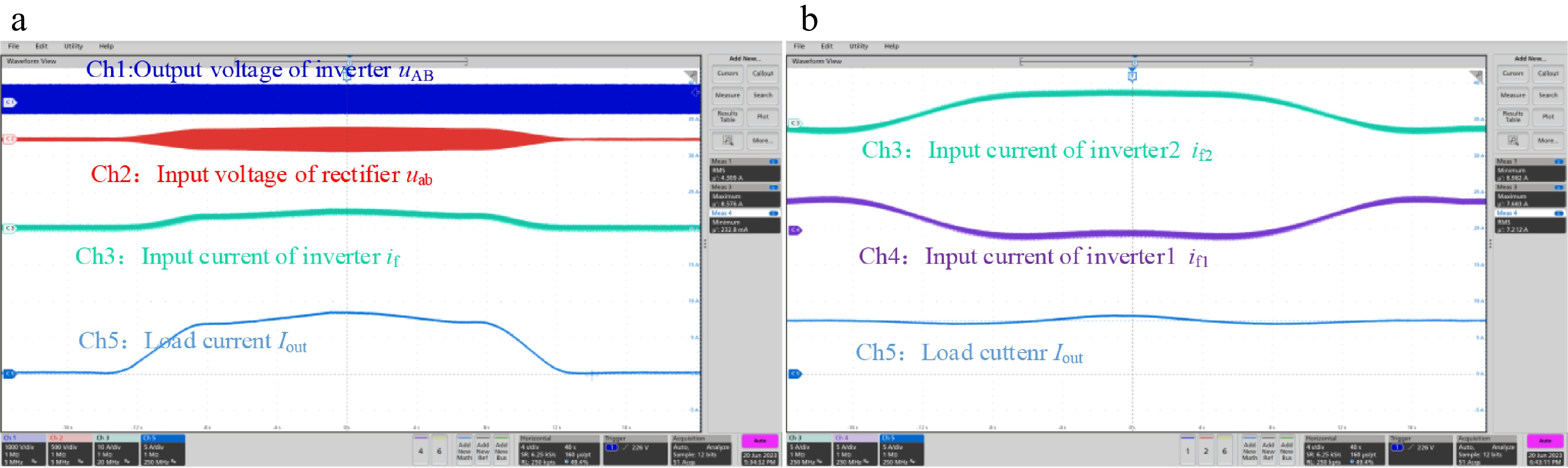
Figure 24.
Output power fluctuation waveforms of CLC-S compensated DWPT system: (a) SISO, (b) DISO.
-
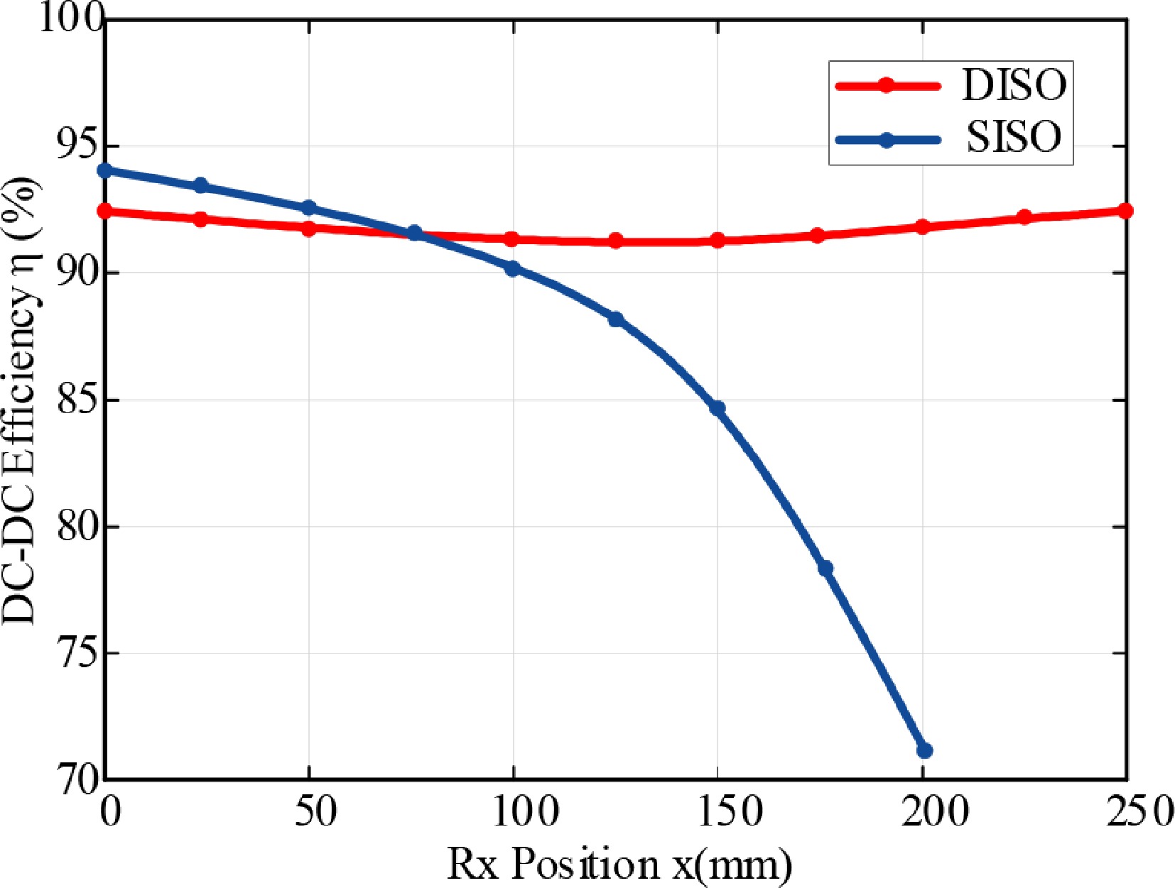
Figure 25.
Comparison of the measured DC-DC efficiency curves between the SISO and DISO systems vs receiver position x.
-
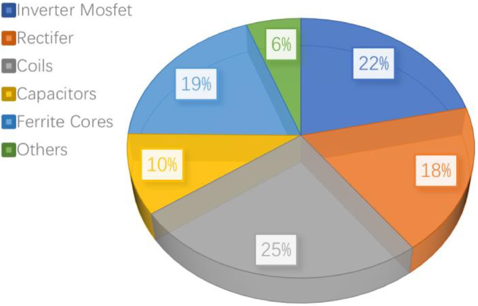
Figure 26.
Loss distribution of the DISO prototype.
-
Symbol Value Symbol Value t1 2 mm FEL 150 mm t2 12 mm FEW 150 mm t3 2 mm ALL 200 mm t4 12 mm ALW 200 mm aL> 100 mm μ0 4π × 10−7 N/A2 aW 100 mm μ1 (μ4) 1.000021 hgap 90 mm μ2 (μ3) 2,300 z1 1.5 mm σ0 0 S/m z2 61.5 mm σ1 (σ4) 3.8 × 10⁷ S/m z3 63 mm σ2 (σ3) 0.1538 S/m n1 15 Table 1.
Pre-fetched parameters of the Tx coil.
-
Order Root mean square value Order Root mean square value 1 5.34 2 2.86 3 1.17 4 0.66 5 0.38 6 0.25 7 0.10 8 0.08 9 0.06 10 0.06 Table 2.
Root mean square values of the Fourier series of different orders.
-
Symbol Value Symbol Value a0 7.827 a1 1.129 a2 1.148 a3 9.223 × 10⁻² a4 −0.7381 a5 −0.5092 a6 1.439 × 10⁻² a7 0.1055 b1 1.413 × 10⁻¹⁷ b2 −1.750 × 10⁻¹⁸ b3 1.198 × 10⁻¹⁶ b4 2.669 × 10⁻¹⁸ b5 1.864 × 10⁻¹⁷ b6 2.497 × 10⁻¹⁷ b7 −8.257 × 10⁻¹⁸ ω 4.102 × 10⁻³ Table 3.
7th order fourier series coefficients.
-
Symbol Value Symbol Value t1 2 mm bL 100 mm t2 12 mm bW 100 mm aL 250 mm n2 15 αw 100 mm hgap 90 mm n1 15 $\varphi _i $ 455 mm Table 4.
Magnetic coupler design parameters.
-
Description FEA Measurement Self-inductance of Tx coil 1 L1 230.86 μH 222.16 μH Self-inductance of Tx coil 2 L2 231.03 μH 226.54 μH Self-inductance of Tx coil 3 L3 230.75 μH 225.49 μH Self-inductance of Rx coil 0 L0 105.26 μH 101.68 μH Same side mutual inductance M12 −20.63 μH −20.91 μH Same side mutual inductance M23 −20.83 μH −21.82 μH Cross-coupling mutual inductance M01 −2.96 μH −3.53 μH Cross-coupling mutual inductance M02 26.39 μH 26.09 μH Cross-coupling mutual inductance M03 −2.91 μH −3.65 μH Table 5.
Comparison of simulated and actual electrical parameters of the magnetic coupler.
-
Symbol Value Symbol Value f 85 kHz C1 13.44 nF R0 25 Ω C2 13.42 nF Lf1 58.62 μH C3 13.42 nF Lf2 60.01 μH Cf1 58.80 nF Lf3 59.95 μH Cf2 58.43 nF C0 34.04 nF Cf3 58.48 nF Table 6.
Some important external circuit parameters.
Figures
(26)
Tables
(6)