-

Figure 1.
Schematic diagram of energy storage and release application.
-
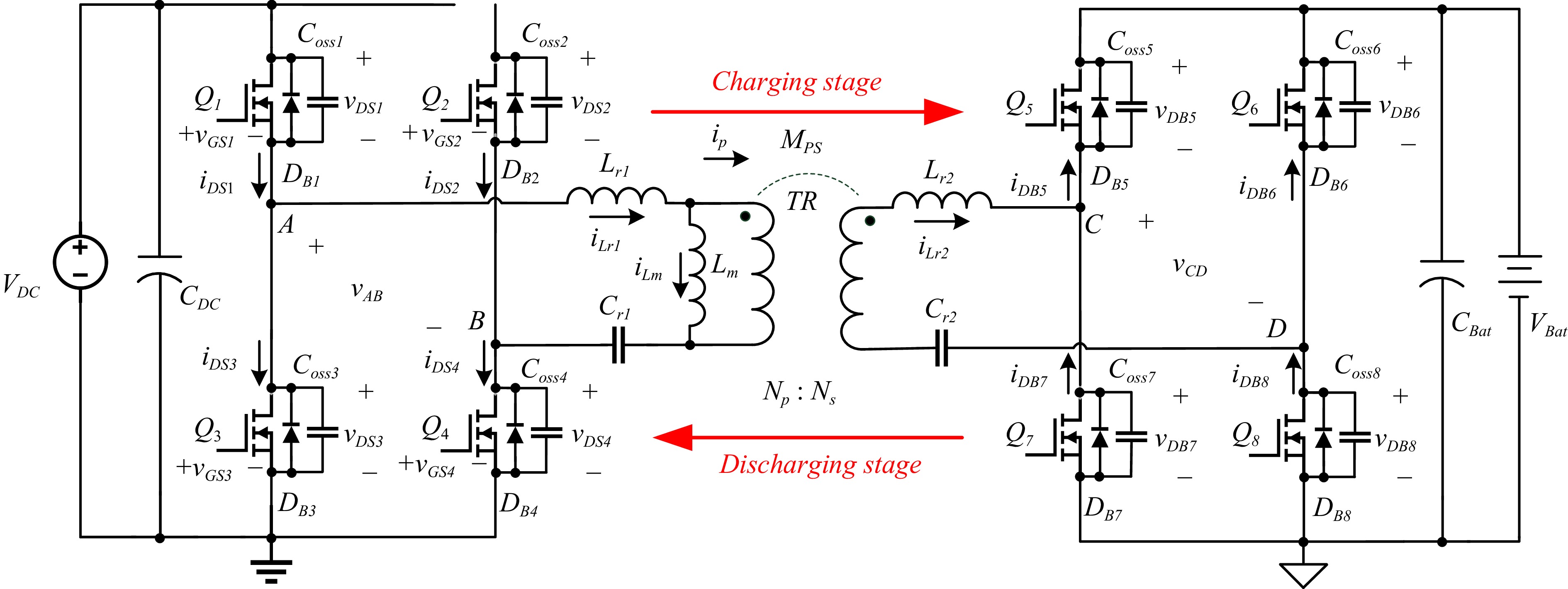
Figure 2.
Circuit diagram of contactless bidirectional energy transmission converter.
-

Figure 3.
Schematic diagram of inductive wireless transmission.
-
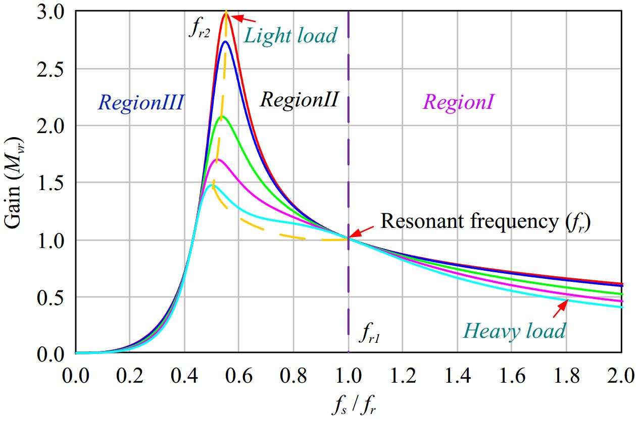
Figure 4.
Bidirectional voltage gain characteristic curve.
-
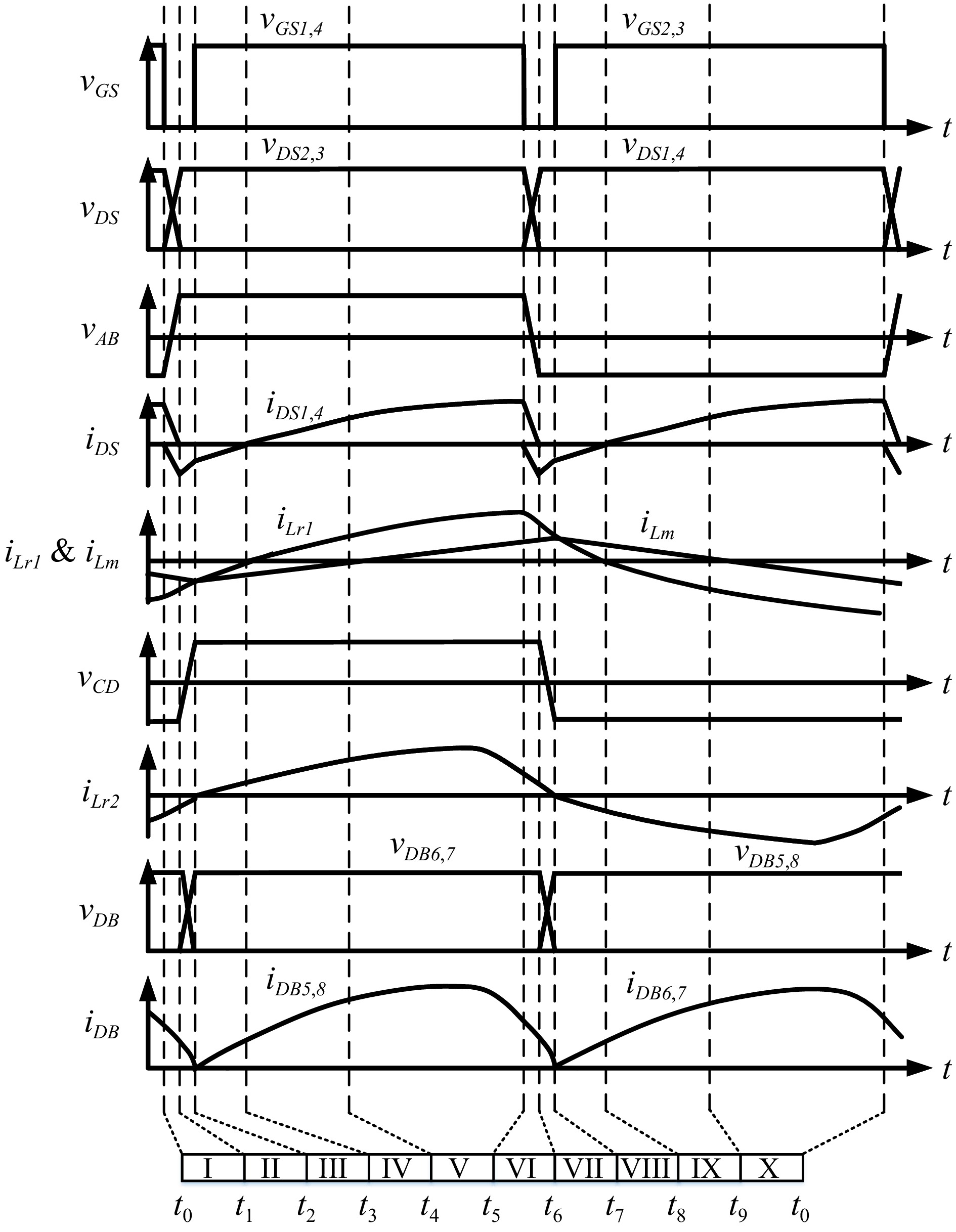
Figure 5.
Theoretical waveform diagram of main components of RegionI (fs > fr1).
-
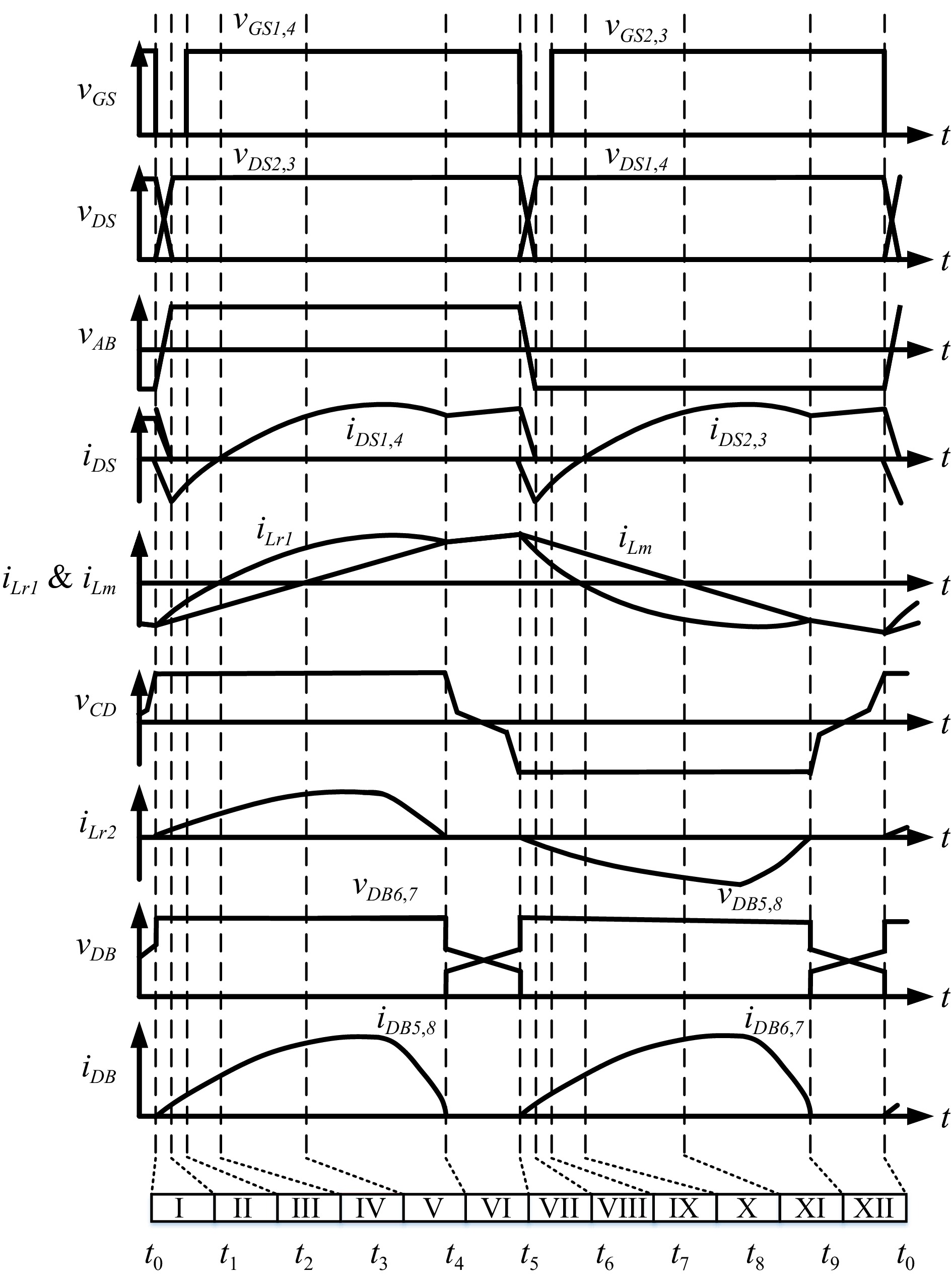
Figure 6.
Theoretical waveform diagram of main components of RegionII (fr2 < fs < fr1).
-
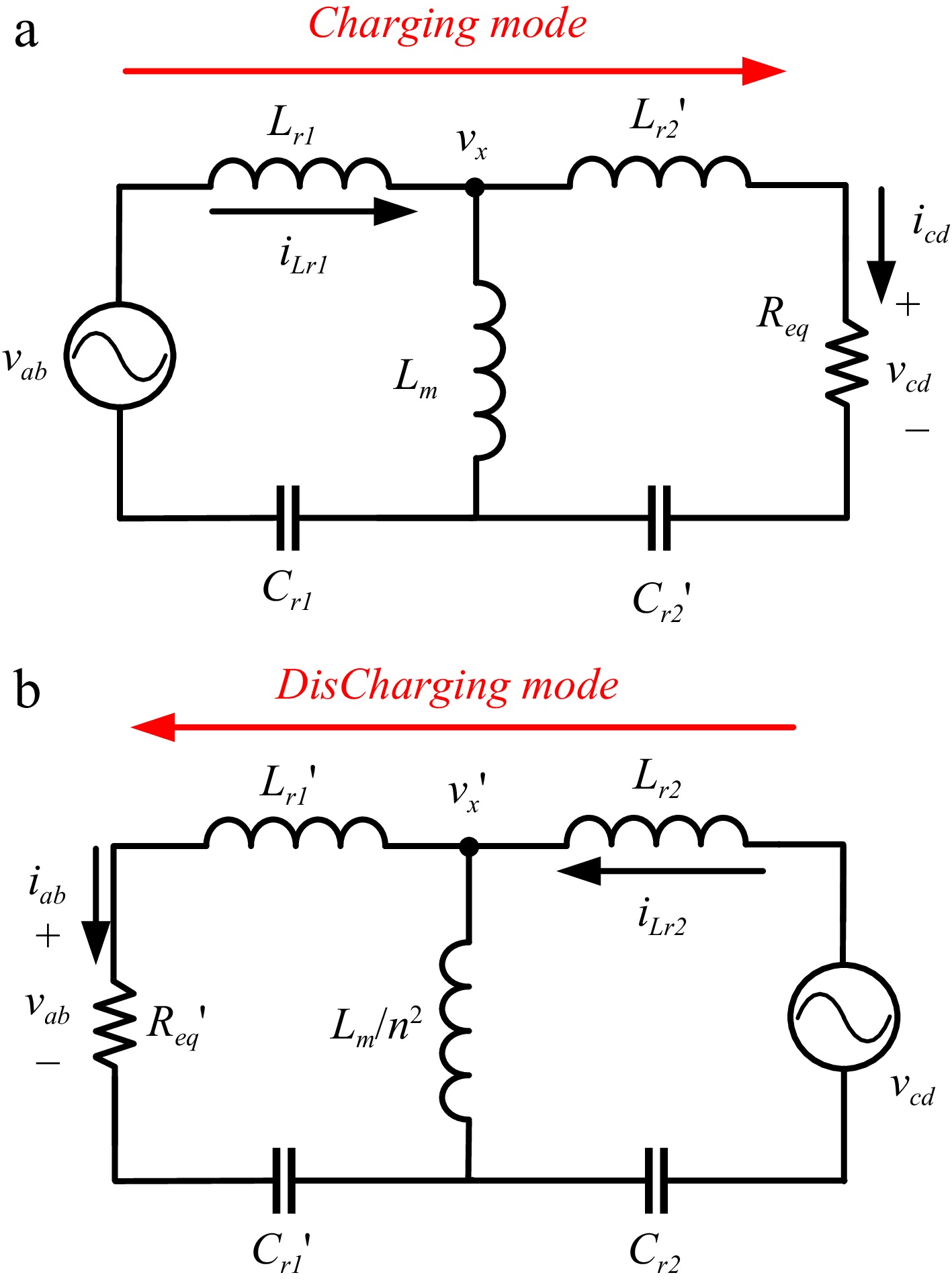
Figure 7.
FHA models of bidirectional resonant converter. (a) Charging stage. (b) Discharging stage.
-
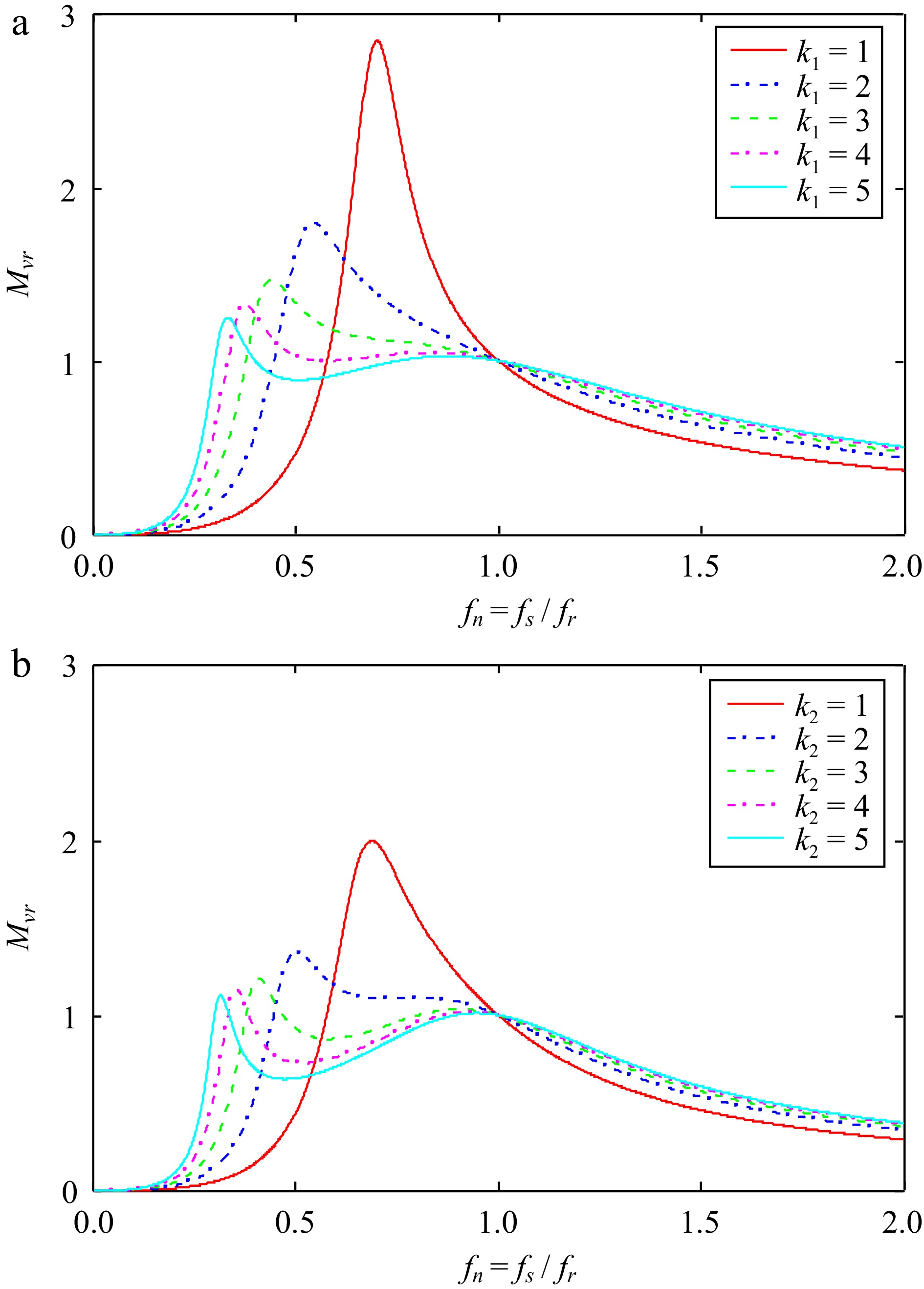
Figure 8.
(a) and (b) voltage gain curves for different k2 values in the charging and discharging mode. (a) Different k1 values in the charging mode. (b) Different k values in the discharging mode.
-
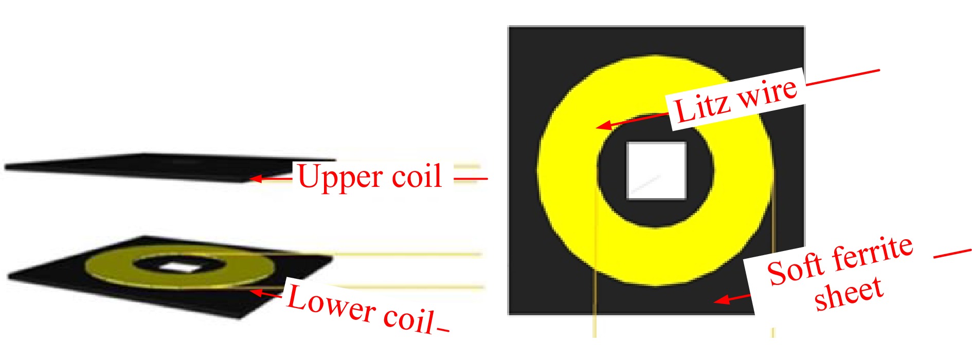
Figure 9.
Schematic of the coil disk.
-
Figure 10.
Wireless coil pair without ferrite sheet.
-
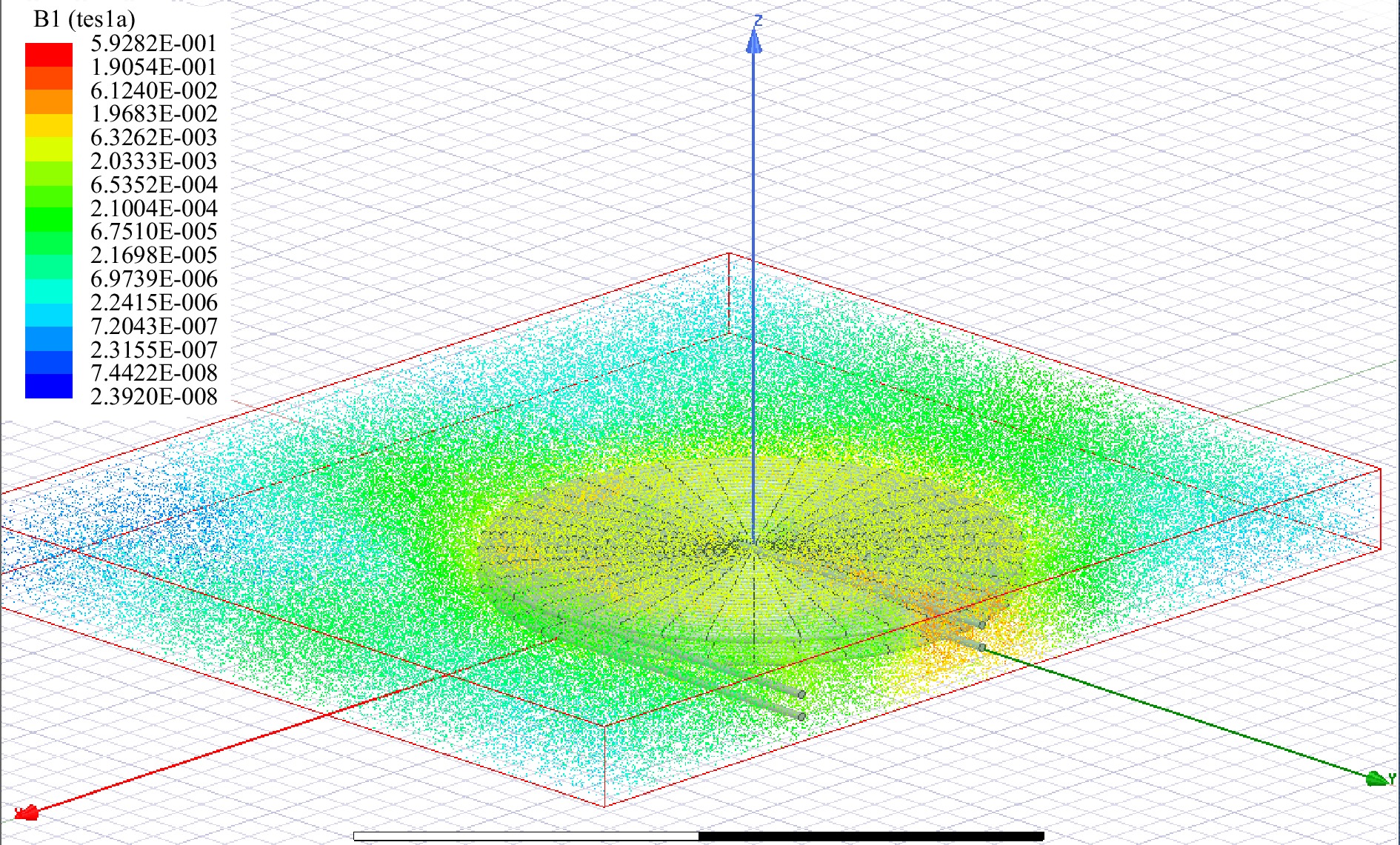
Figure 11.
Magnetic flux distribution of wireless coil pair without ferrite sheet.
-
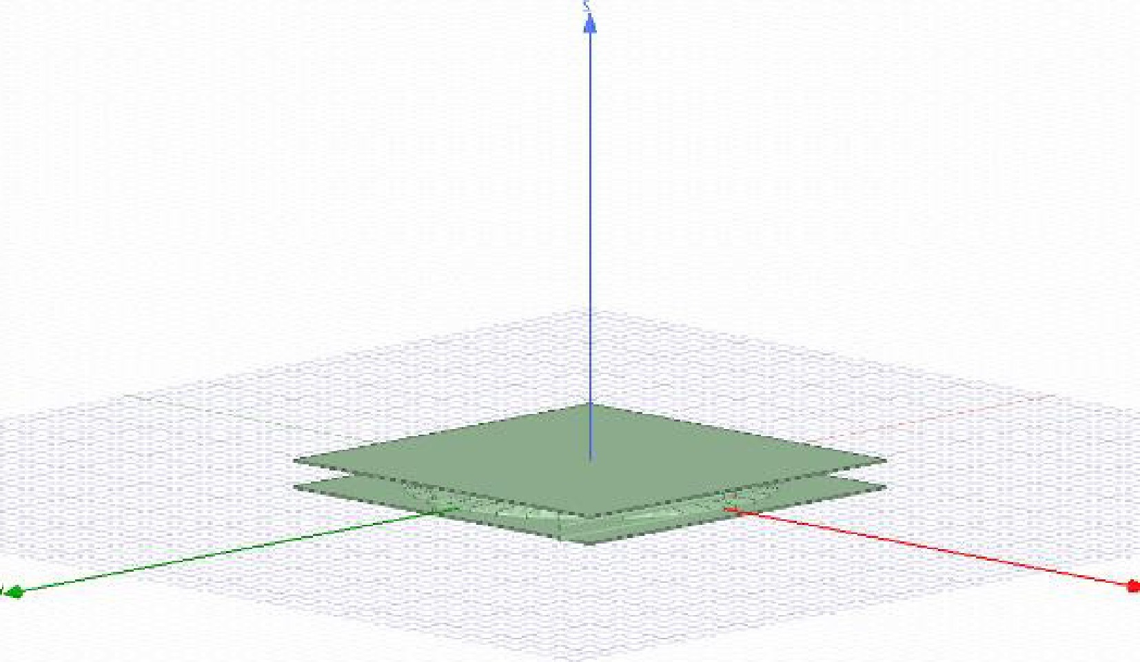
Figure 12.
Wireless coil pair with ferrite sheet.
-
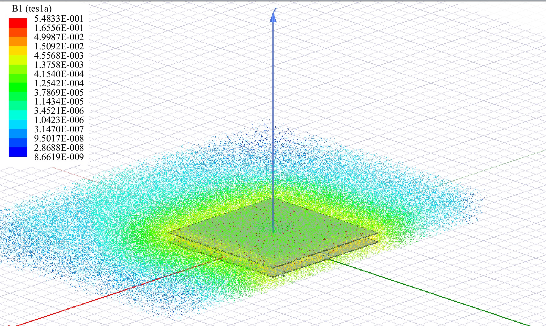
Figure 13.
Magnetic flux distribution of wireless coil pair with ferrite sheet.
-
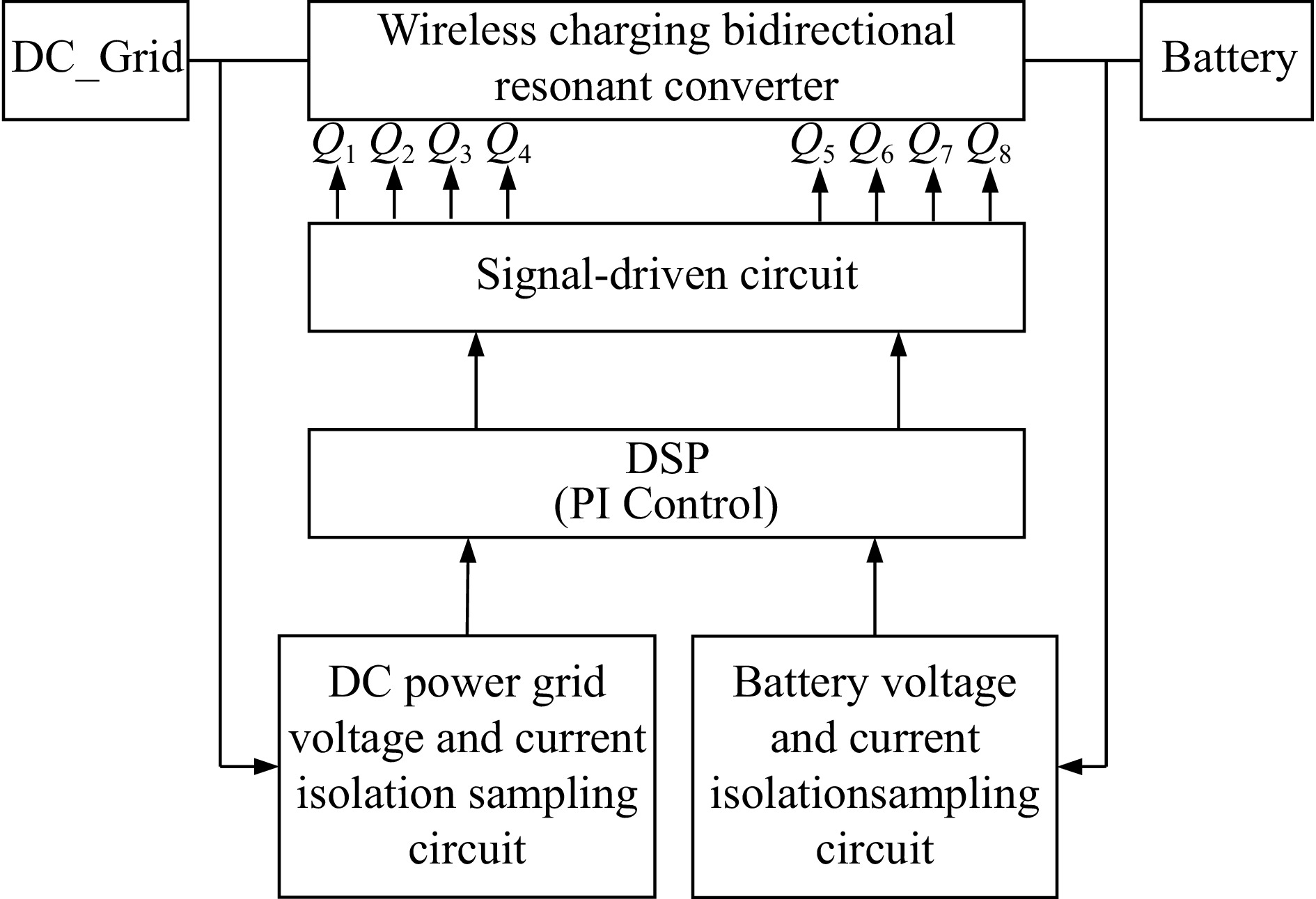
Figure 14.
Converter control architecture diagram.
-
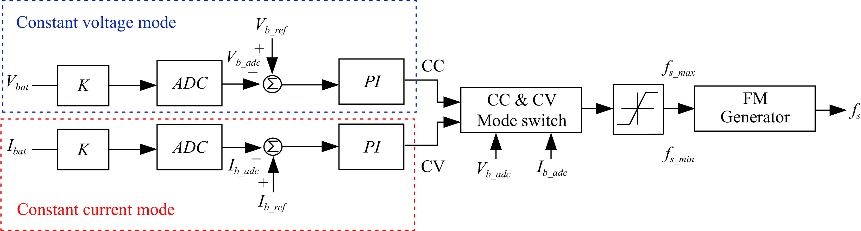
Figure 15.
Block diagram of positive charging storage and release battery terminal feedback system.
-
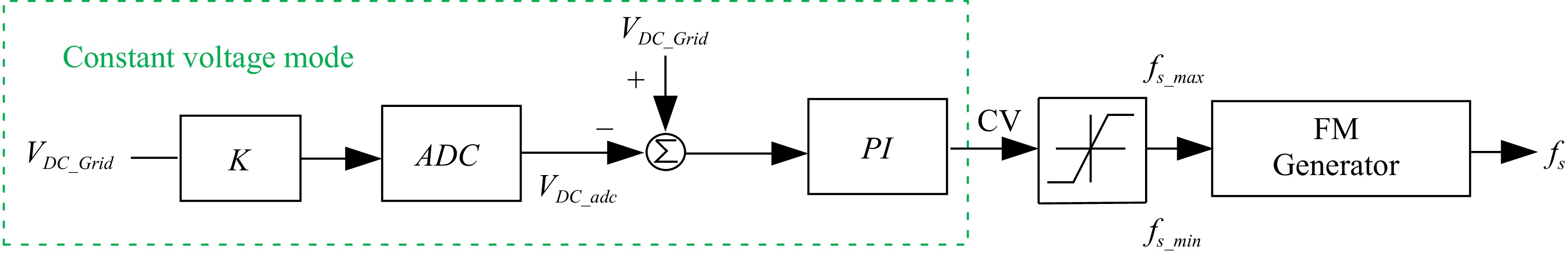
Figure 16.
Block diagram of DC grid end feedback system for reverse discharge.
-
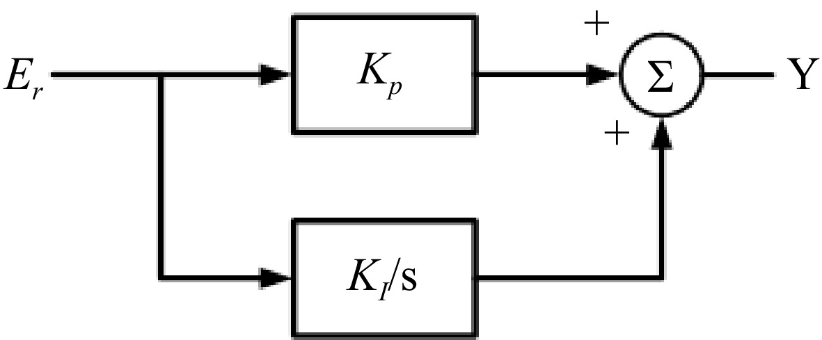
Figure 17.
PI controller block diagram.
-
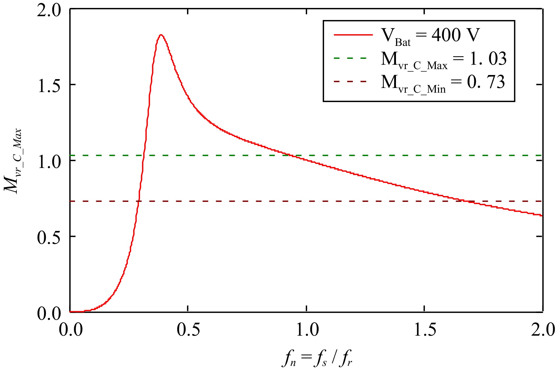
Figure 18.
Initial design of the charging mode gain curve.
-
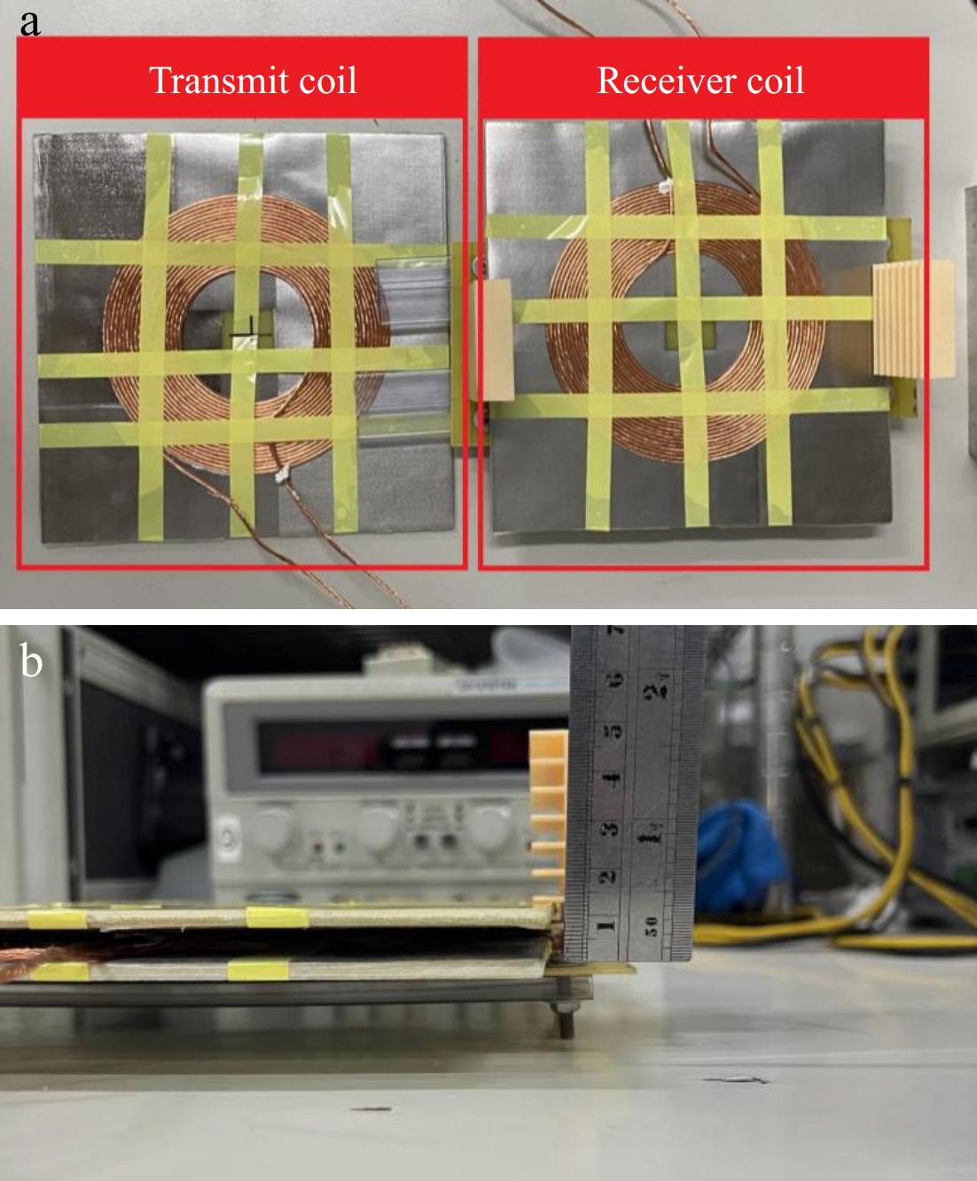
Figure 19.
Practical wireless coil pair. (a) Transmit coil and receiver coil. (b) Non-contact adjustable distance wireless coil pair.
-
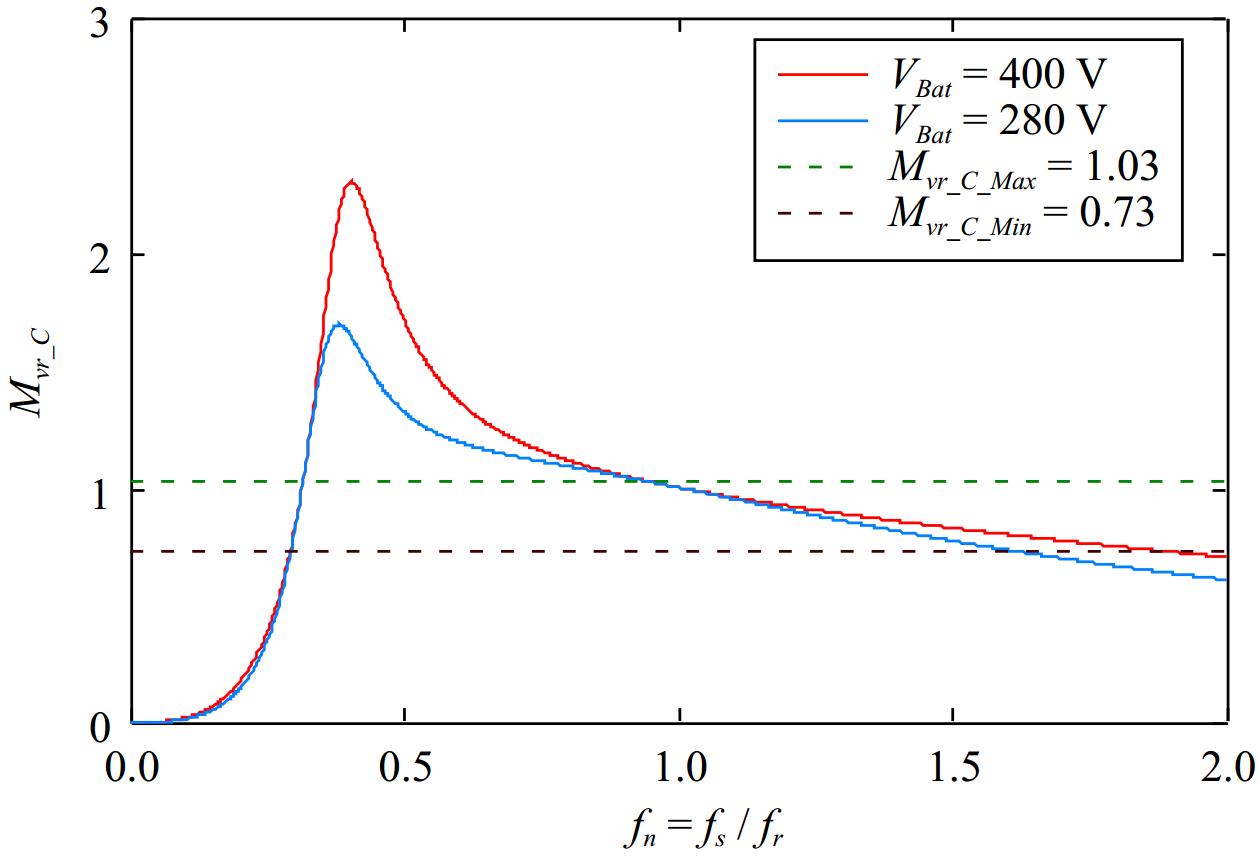
Figure 20.
The design of revised positive voltage gain curves.
-
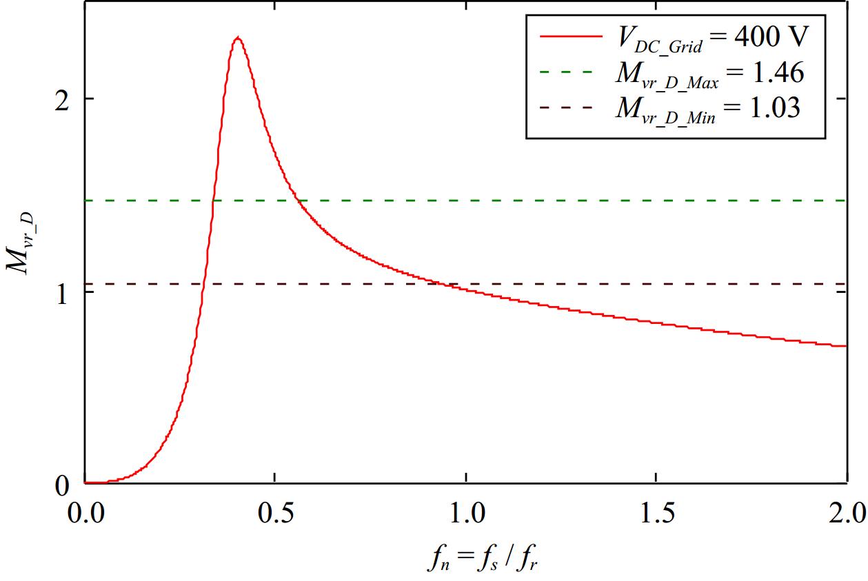
Figure 21.
Design of the discharging mode voltage gain curve.
-
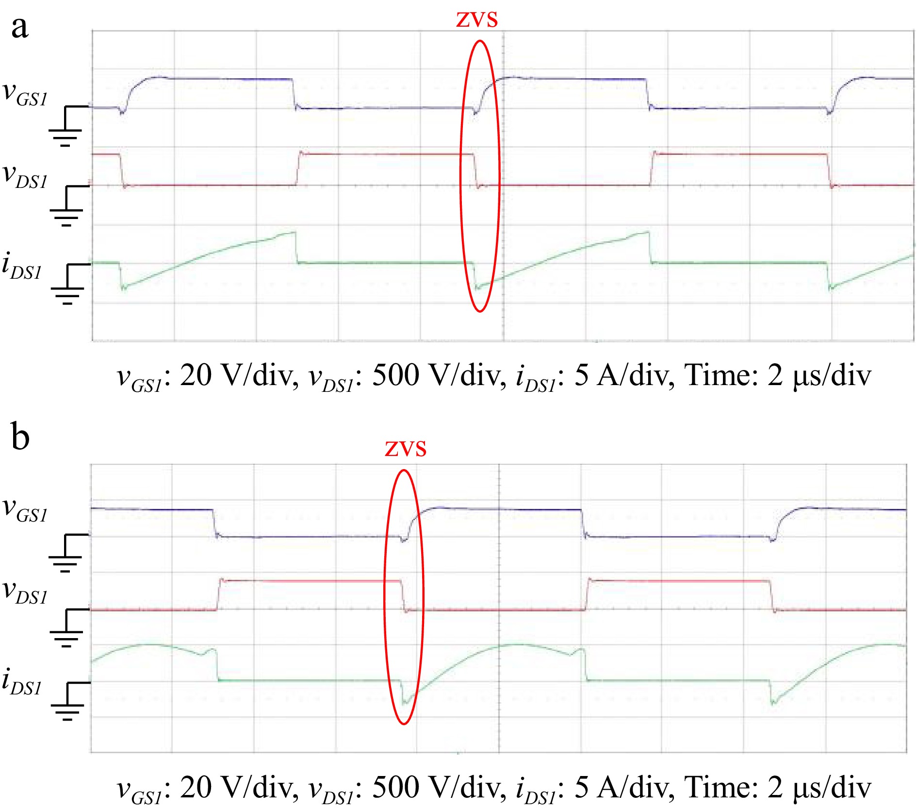
Figure 22.
Various waveforms of power switch Q1 with output current of (a) 0.5 A, and (b) 2.5 A in forward charging CV mode. (a) VDC_Grid = 400 V, VBat = 400 V, IBat = 0.5 A. (b) VDC_Grid = 400 V, VBat = 400 V, IBat = 2.5 A.
-
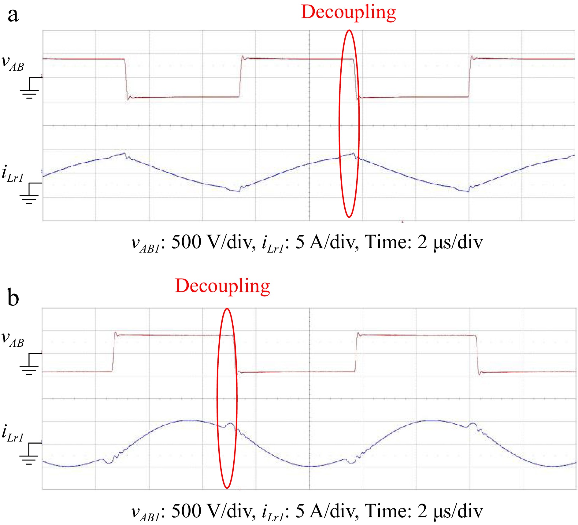
Figure 23.
Waveform of vAB and iLr1 under (a) 0.5 A, and (b) 2.5 A output current of forward charging CV mode. (a) VDC_Grid = 400 V, VBat = 400 V, IBat = 0.5 A. (b) VDC_Grid = 400 V, VBat = 400 V, IBat = 2.5 A
-
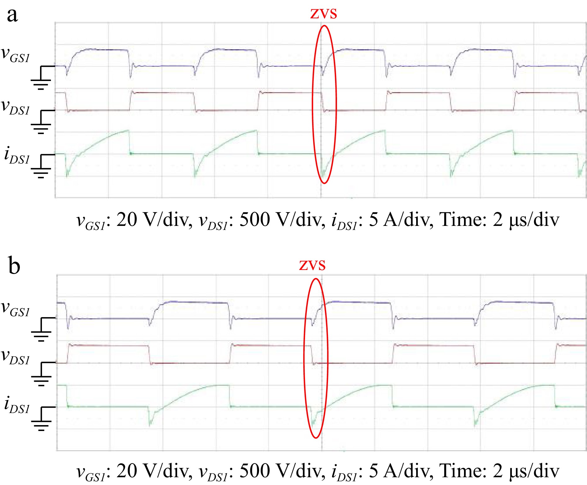
Figure 24.
Various waveforms of power switch Q1 with output voltage of 280 V and 340 V in forward charging CC mode. (a) VDC_Grid = 400 V, VBat = 280 V, IBat = 2.5 A. (b) VDC_Grid = 400 V, VBat = 340 V, IBat = 2.5 A
-
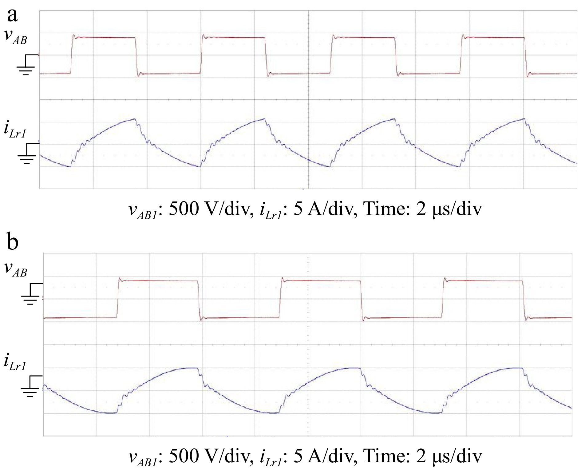
Figure 25.
Waveform of vAB and iLr1 under 280 V, and 340 V output voltage of forward charging CC mode. (a) VDC_Grid = 400 V, VBat = 280 V, IBat = 2.5 A. (b) VDC_Grid = 400 V, VBat = 340 V, IBat = 2.5 A.
-
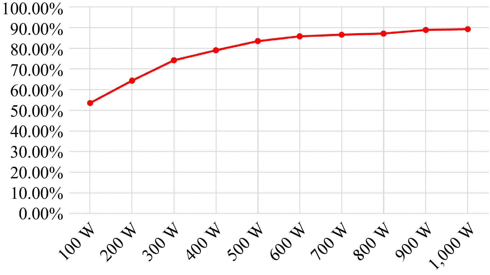
Figure 26.
Efficiency curve for forward charging CV mode.
-
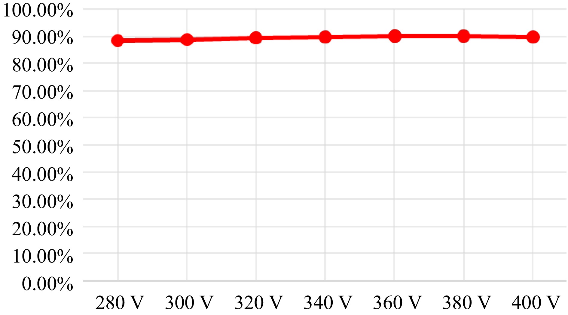
Figure 27.
Efficiency curves for forward charging CC mode with varying output voltage.
-
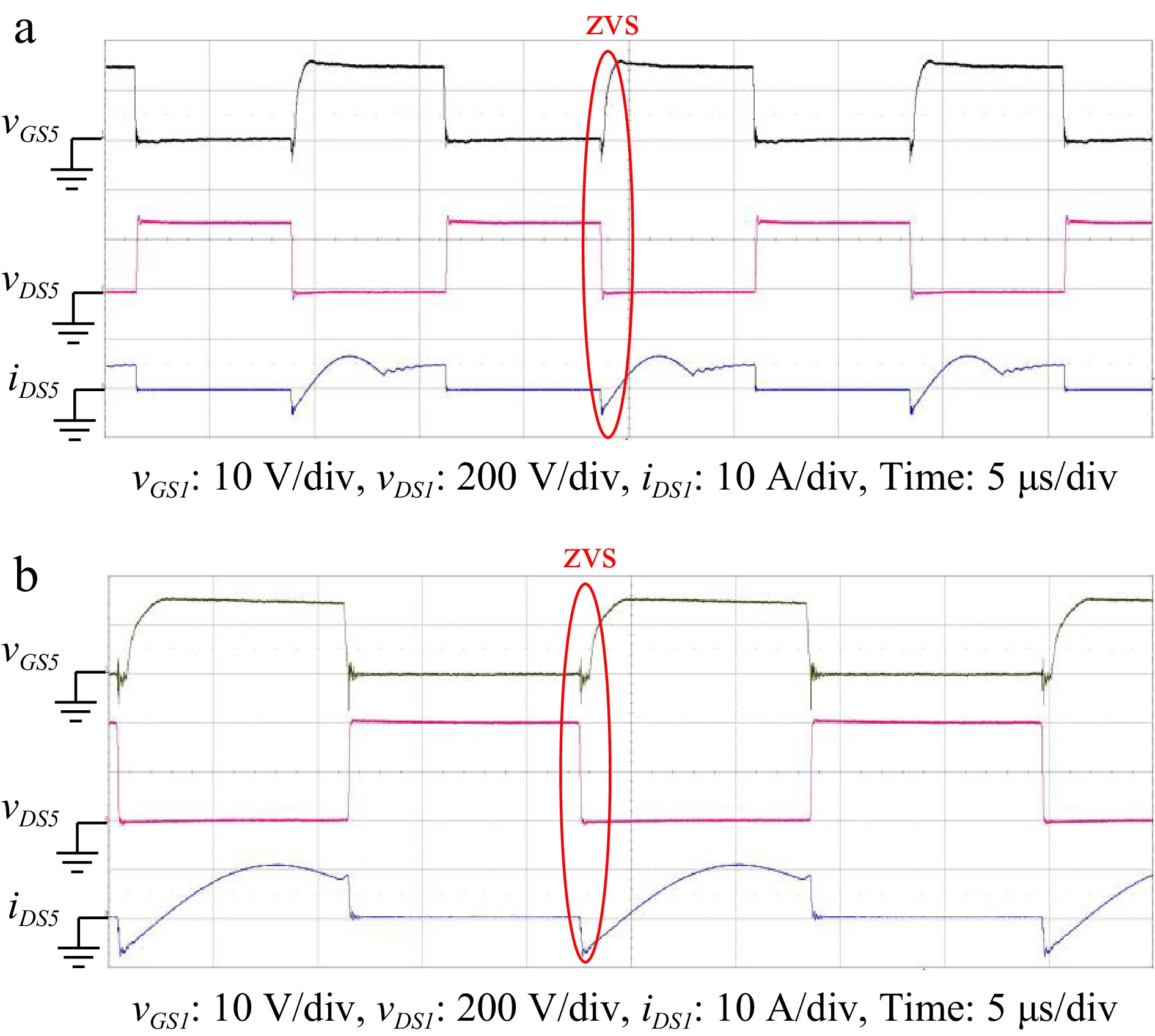
Figure 28.
Various waveforms of power switch Q5 with input voltage of (a) 280 V, and (b) 400 V in reverse discharging. (a) VBat = 280 V, VDC_Grid = 400 V, IBat = 2.5 A. (b) VBat = 400 V, VDC_Grid = 400 V, IBat = 2.5 A.
-
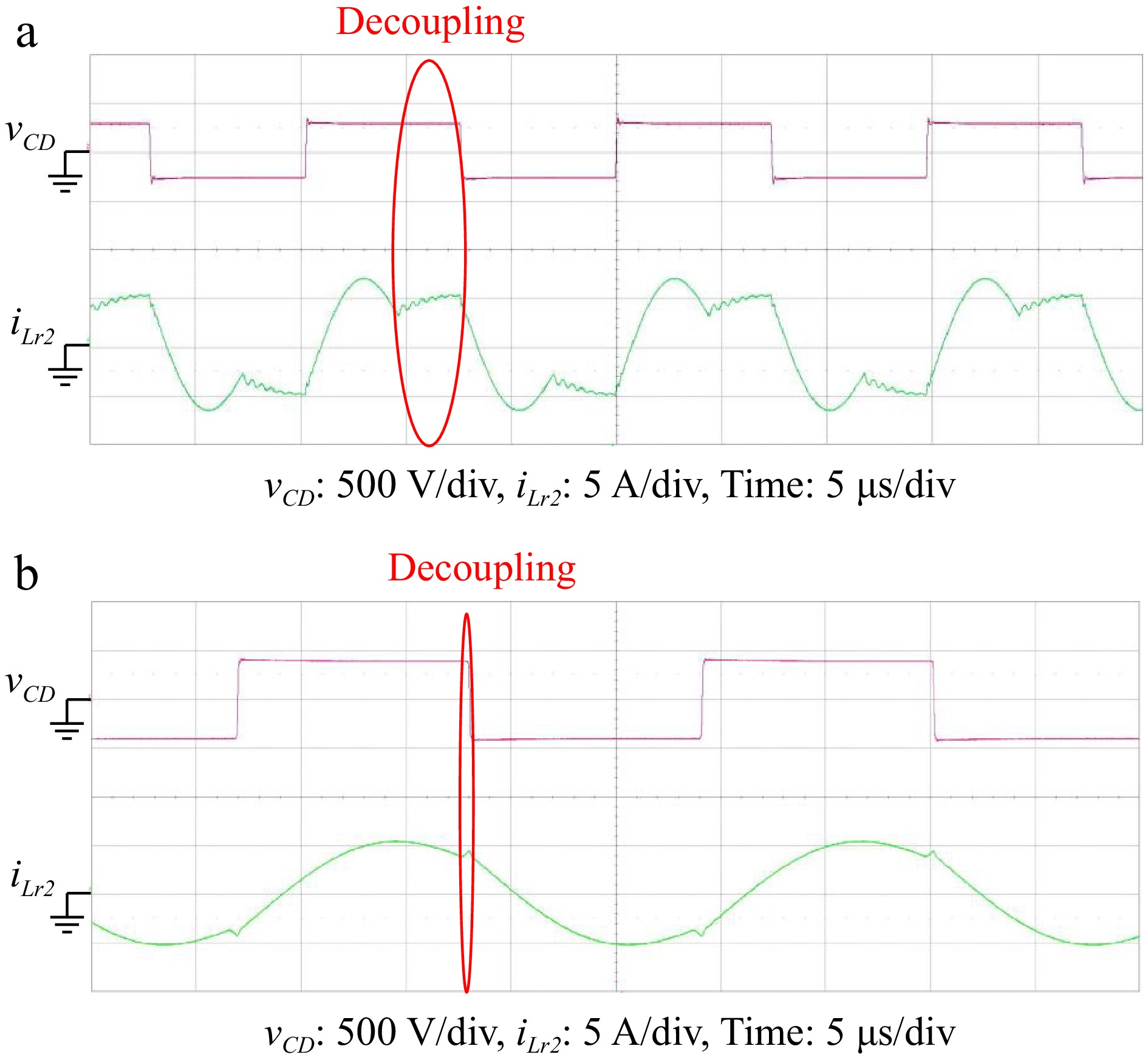
Figure 29.
Waveform of vCD and iLr2 under (a) 280 V, and (b) 400 V battery voltage of reverse discharging. (a) VBat = 280 V, VDC_Grid = 400 V, IBat = 2.5 A. (b) VBat = 400 V, VDC_Grid = 400 V, IBat = 2.5 A.
-
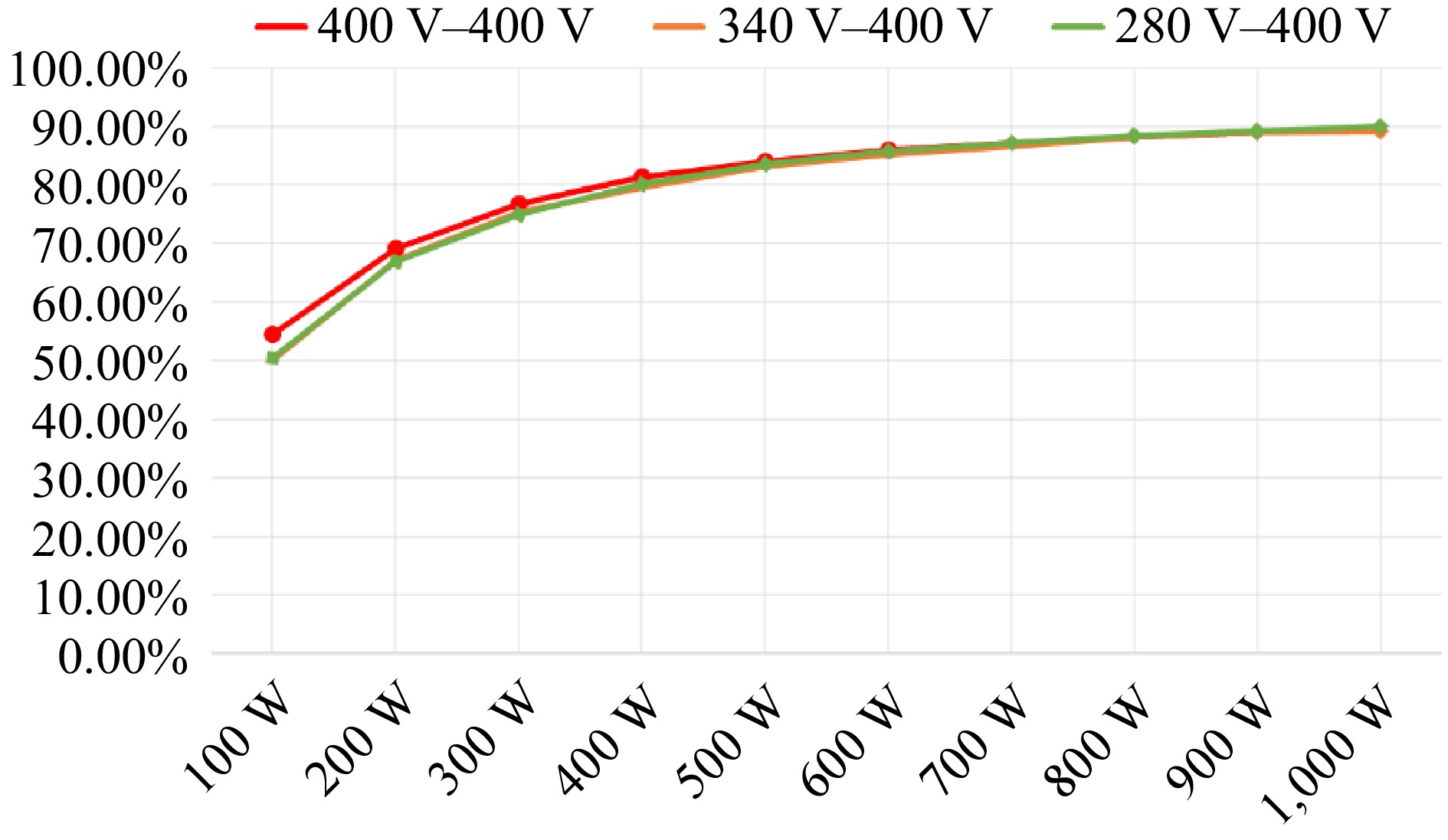
Figure 30.
Efficiency curve of each load under different input voltage in reverse discharging mode.
-
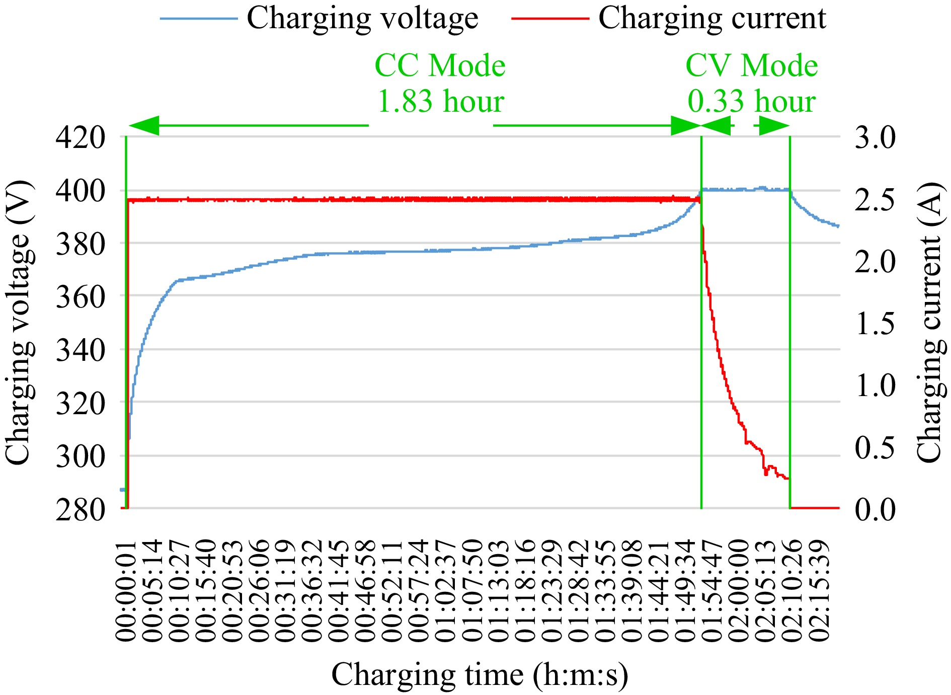
Figure 31.
CC-CV charging voltage-current curve.
-
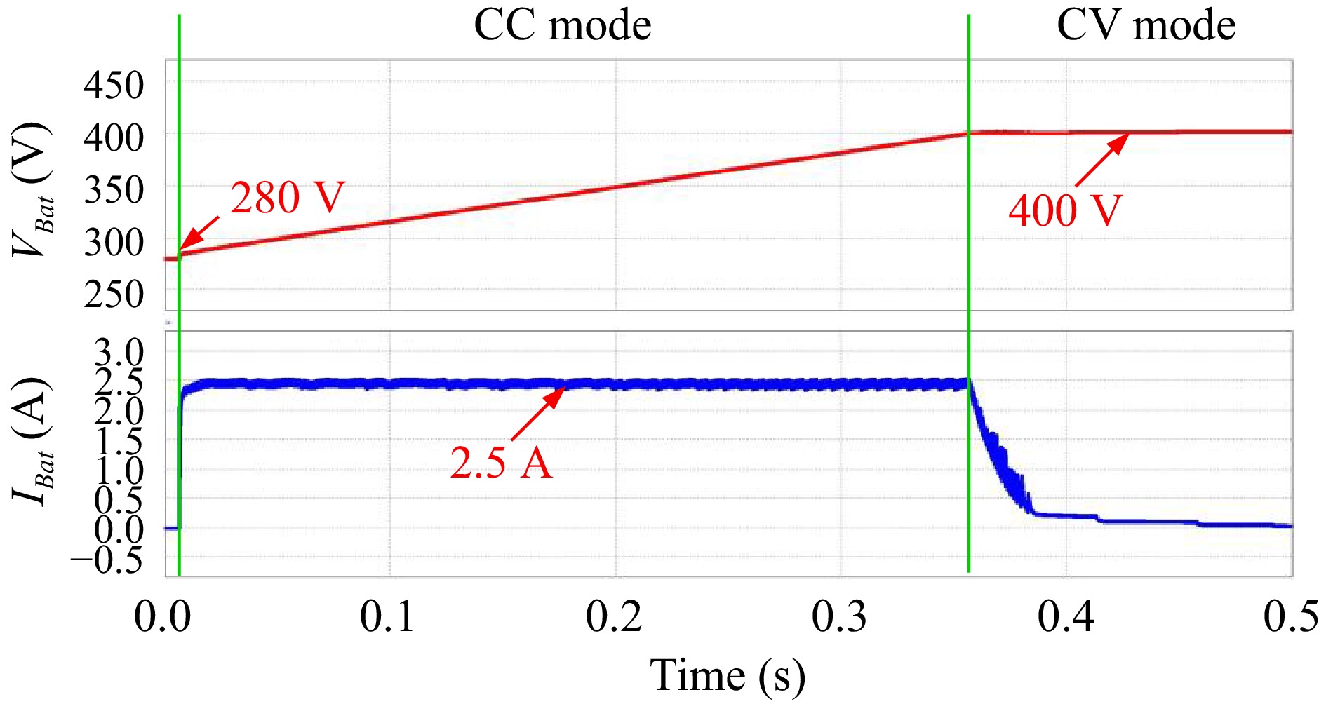
Figure 32.
CC-CV charging state simulation.
-
Parameters Value DC grid voltage (VDC_Grid) 400 V Battery voltage (VBat) 280−400 V Maximum output current (IBat and Idc) 2.5 A Resonant frequency (fr) 100 kHz Table 1.
The specification of the proposed EV charger.
-
Without ferrite sheet Turns 10 20 30 Inductance 2.3 μH 6.1 μH 11 μH With ferrite sheet Turns 10 20 30 Inductance 50 μH 288.5 μH 700.6 μH Table 2.
Comparison table of magnetic field simulation analysis data.
-
Air-gap distance (mm) Lm1 (μH) Lr1 (μH) Lm2 (μH) Lr2 (μH) 1 269.4 14 267.4 13.85 10 213.45 27.11 211.65 26.75 20 120.35 60.38 119.25 59.84 Table 3.
Test of changing coupling air-gap distance of wireless coil pair.
-
Parameters Value Transformer turns-ratio (Np : Ns) 1:1 Magnetizing inductance (Lm) 213.5 μH DC grid side resonant inductance (Lr1) 46.7 μH Battery side resonant inductance (Lr2) 46.1 μH DC grid side resonant capacitance (Cr1) 52 nF Battery side resonant capacitance (Cr2) 52 nF Filter capacitance (CDC_Grid) 540 μF Filter capacitance (CBat) 540 μF Power switches (Q1~Q8) UJ3C065080K3S Digital controller (Dsp) TMS320F28335 Table 4.
Key circuit parameters.
-
Instrument name Model DC power supply Chroma 62024P-600-8 Programmable DC electronic load Chroma 63202 Oscilloscope LeCroy HDO4034 Oscilloscope LeCroy 64Xi Voltage differential probes CYBERTEK DP6150A Current probes CYBERTEK CP8030A Power analyzer PM1000+ Battery recorders MIDI LOGGER GL800 Table 5.
Experimental and measurement instrumentation.
-
Parameters Value Lowest voltage 280 V Standard voltage 369.6 V Recommend charging voltage 400 V Capacity 5.2 Ah Impedance 336 mΩ Energy 1.85 kWh Table 6.
Battery specifications.
Figures
(32)
Tables
(6)