


-
At present, due to the rise in environmental awareness and energy shortage, according to previous research[1−3] that the AC/DC power grid, renewable energy and energy storage and release ports are required, to effectively use the excess electric energy supplied or generated from natural resources for energy storage and release application through a bidirectional converter. The architectural concept is shown in Fig. 1 which has been adapted from previous research studies[4−6], and the concepts of V2G and G2V are adopted in the energy storage and release port. The electric vehicle is used as a movable energy storage and release device to effectively utilize and store electric energy.

Figure 1.
Schematic diagram of energy storage and release application.
In electric energy transmission, this study uses wireless power transmission[7−9], which has the advantages that it can be used in closed devices, avoid exposure of electronic contact ends, and transfer electric energy in different environments. Therefore, it has less restrictions on the environment and climate. On the whole, it has the advantages of safety, reliability, low maintenance cost, and long product life for the transmission device and receiving products, In addition to the convenience brought by wireless transmission, this study will be combined with a bidirectional power converter and inductive wireless transmission to achieve bidirectional wireless power and energy transmission.
Wireless transmission technologies for applications can be broadly categorized into two types: magnetic induction and magnetic resonance. The advantage of magnetic resonance lies in its ability to support multiple power outputs, with the distance between the transmitting and receiving coils capable of achieving energy transfer over distances of 150 to 300 mm or even further. This technology is better suited for charging multiple devices simultaneously compared to magnetic induction. However, due to the high operating frequencies of resonance reaching the MHz range, it is sensitive to frequency variations, which complicates circuit control. Additionally, the potential hazards and impacts of high-frequency, high-power transmission on the human body and surrounding electronic devices remain topics for discussion, contributing to the limited widespread adoption of this technology.
Magnetic induction is currently the most widely used wireless transmission technology. Its advantages include higher efficiency and lower development costs for short-range transmission compared to other wireless charging technologies, and it can be applied across various power levels. However, it is more susceptible tophysical limitations, resulting in shorter transmission distances and potential overheating of the coils, necessitating energy delivery within a specific range. Furthermore, given its characteristics similar to conventional transformer inductance, considerations regarding the design size and weight of the coils must be accounted for, leading to significant design considerations in practical applications[10,11]. In recent years, various compensation circuits have been proposed to mitigate overheating and distance issues, yet there are still various limitations associated with theirarchitecture.
-
In this study, the bidirectional symmetric resonant network is used as the energy storage and release conversion architecture, as shown in Fig. 2. The circuit has a double-active symmetrical full bridge power switch and a symmetrical resonant tank. Its characteristics are similar to the two-way LLC resonant converter. To improve the disadvantage that LLC cannot adjust the voltage in a wide range during two-way operation, a resonant element is added on the load side. Its resonant loop is composed of Cr1, Lr1, Lm, Lr2, and Cr2. In addition, it interacts with Q5−Q8 through Q1−Q4, a bidirectional wide-range voltage load conversion architecture is formed[12−14].
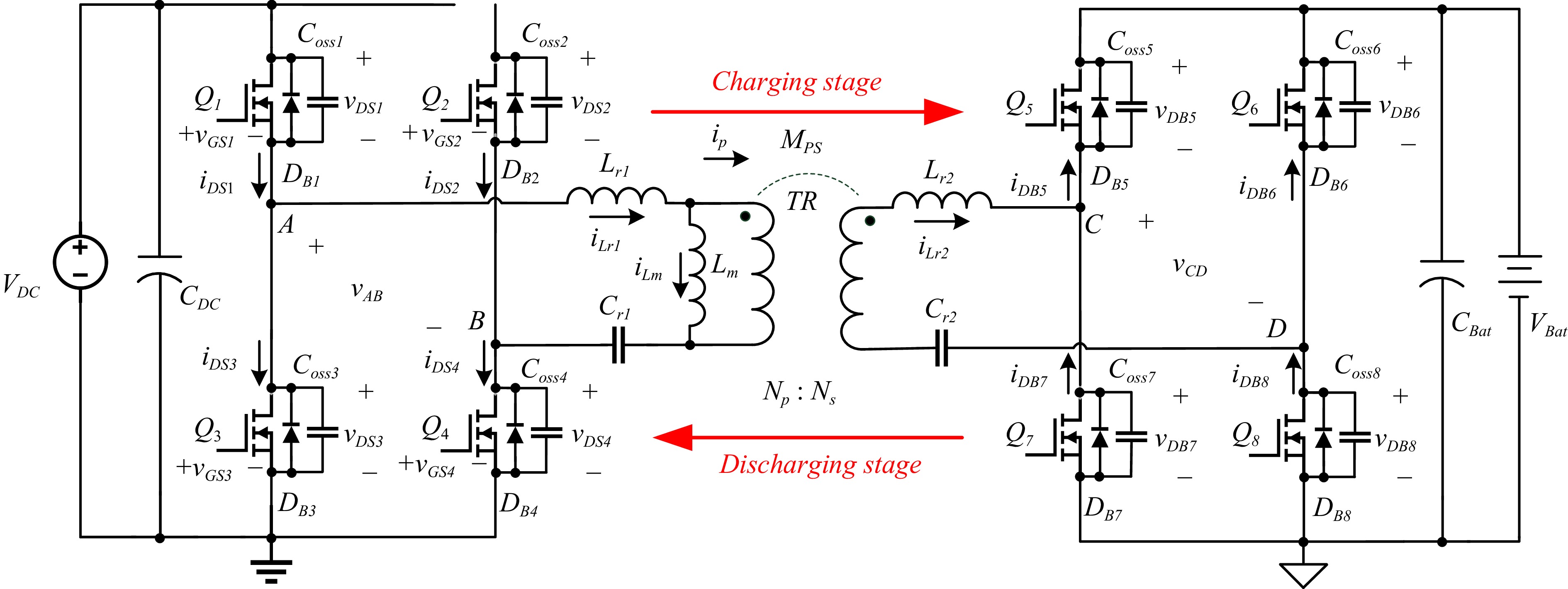
Figure 2.
Circuit diagram of contactless bidirectional energy transmission converter.
During the circuit operation, the power switches can be divided into a controlled side and a rectifier side according to its function. The switches on the controlled side are used as a full bridge inverter, which cuts the DC input voltage into square waves, and the body diode within the switches on the rectifier side are used as a rectifier to rectify the AC voltage into DC voltage output. With bidirectional power transmission, the function of wide-range soft switching of power switch can be achieved without adding additional circuits, so as to reduce switching loss and EMI interference.
In the part of energy wireless transmission, this study adopts inductive coupling wireless transmission[15−17]. Similar to the traditional transformer, the transmitting coil uses the coupling magnetic line of force to transmit the energy to the receiving coil. Therefore, the transmission is affected by the distance, and it is recommended to operate between 0.1−10 mm. Finally, the dual coil is used for wireless transmission in the converter. The transmission diagram is shown in Fig. 3.

Figure 3.
Schematic diagram of inductive wireless transmission.
Analysis of the voltage gain and circuit operation principle
-
Through mathematical operation simulation software, the corresponding voltage gain curve can be drawn according to the design parameters of the bidirectional energy converter, as shown in Fig. 4.
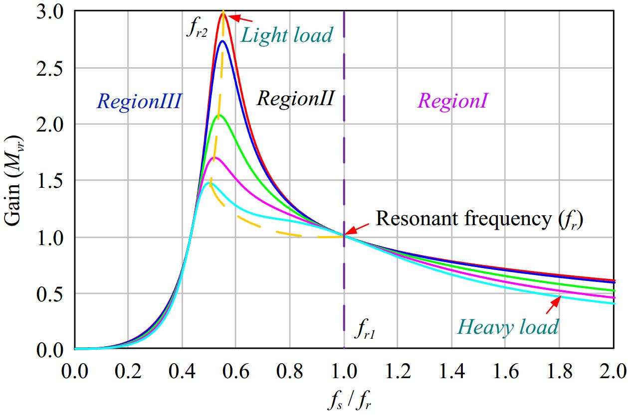
Figure 4.
Bidirectional voltage gain characteristic curve.
The resonance point fr and the second resonance point fr2 can be divided into three intervals, and can be analyzed into the following three working states:
(1) When fs < fr2, the voltage gain curve operates in RegionIII. At this time, the resonant circuit of the converter is capacitive, so that the power switch on the controlled side can't achieve the effect of ZVS, resulting in a large amount of power loss, and the load energy will be injected back to the controlled side in the action process, resulting in switching damage. Therefore, when designing the voltage gain and operating frequency, the converter shall not operate in this range.
(2) When fr2 < fs < fr1, the voltage gain curve operates in RegionII. At this time, the resonant circuit of the converter is inductive, so that the power switch on the controlled side reaches ZVS, and when Lm participates in resonance, the rectifier switch reaches ZCS. This interval can achieve soft switching on both the controlled side and the rectifier side, which is the best interval in design.
(3) When fr1 < fs, the voltage gain curve operates in RegionI. At this time, the resonant circuit of the converter is inductive, and the switch on the controlled side reaches ZVS, but the resonant current and magnetizing current do not have the same current working range, so the rectifier side can't achieve the function of ZCS.
In Fig. 4, frequency modulation for controlling voltage gain can achieve the desired output voltage for CC/CV applications.
This study belongs to bidirectional wide input and output voltage. Considering the above introduction, the converter is operated in RegionI and RegionII for frequency conversion control. The working flow is analyzed in detail below.
Figure 5 shows the theoretical waveform of the converter operating in RegionI. According to the power switch switching and current state, the power switch signal can be divided into 10 groups of modes in a complete cycle. Since the working states of the positive half cycle (I−V) and the negative half cycle (VI−X) are similar, the characteristics of the circuit and ZVS are analyzed in five working modes of the positive half cycle.
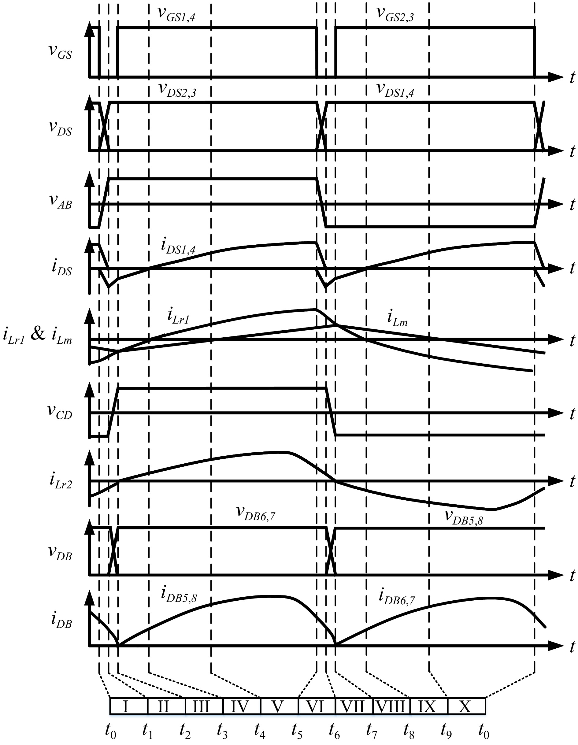
Figure 5.
Theoretical waveform diagram of main components of RegionI (fs > fr1).
Mode I [t0-t1]: At t = t0, the gate signals vGS2 and vGS3 of power switches Q2 and Q3 change from high potential to low potential, and the circuit enters dead time. The resonant current iLr1 maintains the current direction, the parasitic capacitors Coss1 and Coss4 of the power switch release energy through iLr1, and iLr1 stores energy for Coss2 and Coss3. Due to iLr1, and iLm, not being equal, their current difference transmits energy to the secondary side through the TR, which is rectified and output through the essential diodes DB6 and DB7. When the parasitic capacitors Coss1 and Coss4 of the power switch are completely discharged to zero, Coss2 and Coss3 are charged to VDC, and the interval ends.
Mode II [t1-t2]: At t = t1, power switches Q1 ~ Q4 are in off state. The resonant current iLr1 forms a freewheeling path through the essential diodes DB1 and DB4 of the power switch, so that the power switches Q1 and Q4 meet the ZVS condition. At this time, the current difference continuously provides energy to the secondary side, which is rectified and output through the essential diodes DB6 and DB7. At t = t2, gate signals vGS1 and vGS4 change from low potential to high potential, this interval ends.
Mode III [t2-t3]: At t = t2, Q1 and Q4 are on, and the power switch reaches ZVS. At this time, iLr1 is greater than iLm, which changes the flow direction of the resonant current iLr2 on the secondary side. It is rectified and output through the essential diodes DB5 and DB8. Because there is still current passing when the essential rectifier diodes DB6 and DB7 are cut off at t = t2, resulting in hard switching, the rectifier diodes cannot realize ZCS.
Mode IV [t3-t4]: At t = t3, Q1 and Q4 remain on, and the resonant current iLr1 changes from negative to 0. At this time, VDC resonates through Cr1 and Lr1, so that the resonance current iLr1 is not equal to the magnetizing current iLm and its current difference transmits energy to the secondary side through the transformer, which is rectified and output by the essential diodes DB5 and DB8. The magnetizing inductance Lm doesn't participate in the resonance, so the magnetizing current iLm keeps rising linearly. When the magnetizing current iLm = 0, this interval ends.
Mode V [t4-t5]: At t = t4, the flow direction of the magnetizing current iLm changes. At this time, due to the resonant current iLr1 and magnetizing current iLm current difference increases, and energy is transferred to the secondary side through the TR to make the secondary side resonant current iLr2 continues to rise and is rectified and output by intrinsic diodes DB5 and DB8. The magnetizing inductance Lm doesn't participate in the resonance, so the magnetizing current iLm keeps rising linearly.
Figure 6 shows the theoretical waveform of the converter operating in RegionII. According to the power switch switching and current state, the power switch signal can be divided into 12 groups of modes in a complete cycle. Since the working states of the positive half cycle (I−VI) and the negative half cycle (VII−XII) are similar, the characteristics of the circuit and ZVS, ZCS are analyzed in six working modes of the positive half cycle.
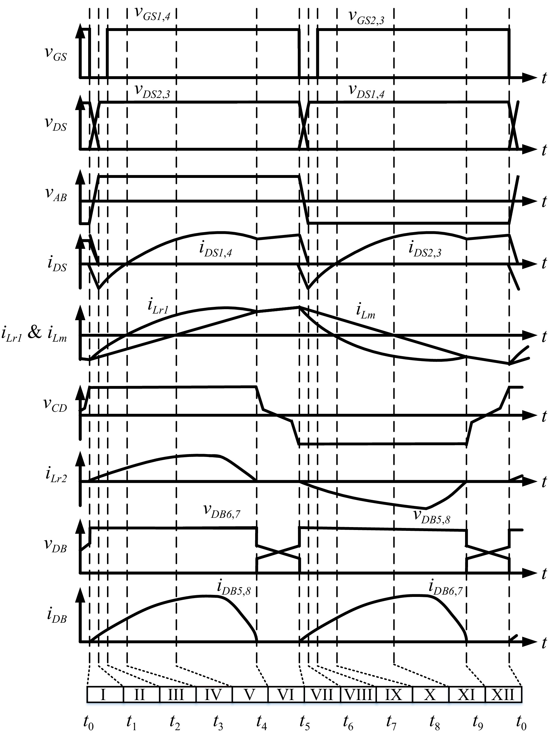
Figure 6.
Theoretical waveform diagram of main components of RegionII (fr2 < fs < fr1).
Mode I [t0-t1]: At t = t0, the gate signals vGS2 and vGS3 of power switches Q2 and Q3 change from high potential to low potential, and the circuit enters dead time. The resonant current iLr1 maintains the current direction, the parasitic capacitors Coss1 and Coss4 of the power switch release energy through iLr1, and iLr1 stores energy for Coss2 and Coss3. Due to iLr1, and iLm, not being equal, and it's current difference transmits energy to the secondary side through the TR, which is rectified and output through the essential diodes DB6 and DB7. When the parasitic capacitors Coss1 and Coss4 of the power switch are completely discharged to zero, Coss2 and Coss3 are charged to VDC, and the interval ends.
Mode II [t1-t2]: At t = t1, power switches Q1 ~ Q4 are in off state. The resonant current iLr1 forms a freewheeling path through the essential diodes DB1 and DB4 of the power switch to avoid the open circuit of the resonant current source, resulting in voltage surge and component damage. At the same time, Q1 and Q4 meet the conditions of ZVS. When t = t2 gate signals vGS1 and vGS4 change from low potential to high potential, this interval ends.
Mode III [t2-t3]: At t = t2, Q1 and Q4 are on, the power switch achieves the function of ZVS. At this time, iLr1 and iLm continue to rise, and their current difference transmits energy to the secondary side through the transformer, which is rectified and output by the essential diodes DB5 and DB5, while the magnetizing inductance does not participate in resonance, so the magnetizing current iLm keeps rising linearly.When t = t3 resonant current iLr1 = 0, this interval ends.
Mode IV [t3-t4]: At t = t3, the power switches Q1 and Q4 remain on, and the resonant current iLr1 changes from negative to 0. At this time, VDC resonates through Cr1 and Lr1 so that the resonant current iLr1 and magnetizing current iLm are not equal, and their current difference transmits energy to the secondary side through TR, which is rectified and output by essential diodes DB5 and DB8. The magnetizing inductance Lm does not participate in the resonance, so the magnetizing current iLm keeps rising linearly. Since the voltage at both ends of Cr1 is increasing, the slope of iLr1 gradually decreases. When the magnetizing current iLm = 0, this interval ends.
Mode V [t4-t5]: At t = t4, the power switches Q1 and Q4 remain on, and the flow direction of magnetizing current iLm changes. At this time, the resonant current iLr1 and magnetizing current iLm current difference increases, and energy is transmitted to the secondary side through TR to make the secondary side resonant current iLr2 continues to rise and is rectified and output by essential diodes DB5 and DB8. iLr1 is affected by resonance and finally decreases continuously when iLr1 is equal to iLm, the interval ends.
Mode VI [t5-t6]: At t = t5, iLr1 and iLm are equal. At this time, the transformer enters the decoupling interval to make iLr2 of zero. Therefore, the secondary side intrinsic diodes DB5 and DB8 naturally reduce the current to zero to achieve ZCS. Since TR enters the decoupling interval, the resonance in this interval is achieved by Lr1, Cr1, and Lm, VDC continuously supplies energy to Lr1 and Lm. When t = t5, the gate signals vGS1 and vGS4 of power switches Q1 and Q4 change from high potential to low potential, power switches Q1 and Q4 cut off and this working stage ends.
Since the resonant converter is controlled by PFM, the operating frequency range is also one of the important considerations in the design process. When operating at the resonant frequency point, the resonant current is similar to a sine wave. Therefore, the bidirectional symmetric resonant converter can be analyzed by the basic harmonic approximation (FHA). Figure 7 shows the simplified equivalent model's forward charge stage and reverse discharge stage.
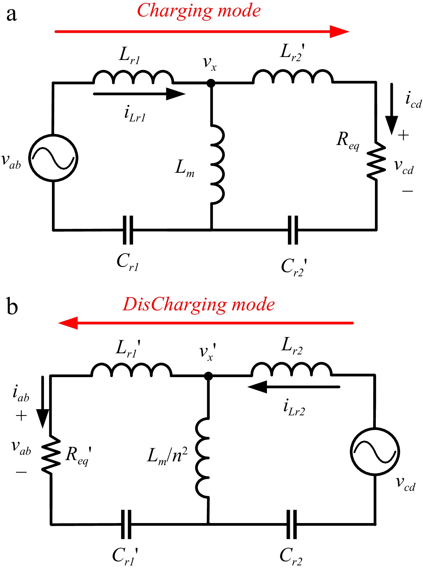
Figure 7.
FHA models of bidirectional resonant converter. (a) Charging stage. (b) Discharging stage.
Since the symmetrical resonant structure is similar to the directional equivalent circuit, the bidirectional voltage gain is obtained by using the voltage division theorem, as shown in Eqn (1) and Eqn (2) below.
$ {M}_{vr\_Charging}=\dfrac{1}{\sqrt{{\left[1+\dfrac{1}{{k}_{1}}-\dfrac{1}{{k}_{1}{\left({f}_{n\text{}\_C}\right)}^{2}}\right]}^{2}+{{q}_{1}}^{2}{\left[\left(1+{h}_{1}+\dfrac{{h}_{1}}{{k}_{1}}\right){f}_{n\text{}\_C}-\dfrac{\left(1+\dfrac{1}{{g}_{1}}+\dfrac{1}{{k}_{1}{g}_{1}}\right)}{{f}_{n\text{}\_C}}+\dfrac{\left(\dfrac{1}{{k}_{1}{g}_{1}}\right)}{{\left({f}_{n\text{}\_C}\right)}^{3}}\right]}^{2}}} $ (1) $ {M}_{vr\_Discharging}=\dfrac{1}{\sqrt{{\left[1+\dfrac{1}{{k}_{2}}-\dfrac{1}{{k}_{2}({{f}_{n\text{}\_D})}^{2}}\right]}^{2}+{{q}_{2}}^{2}{\left[\left(1+{h}_{2}+\dfrac{{h}_{2}}{{k}_{2}}\right){f}_{n\text{}\_D}-\dfrac{\left(1+\dfrac{1}{{g}_{2}}+\dfrac{1}{{k}_{2}{g}_{2}}\right)}{{f}_{n\text{}\_D}}+\dfrac{\left(\dfrac{1}{{k}_{2}{g}_{2}}\right)}{{\left({f}_{n\text{}\_D}\right)}^{3}}\right]}^{2}}} $ (2) In addition, fn is the normalized frequency, q is the defined quality factor, k is the inductance ratio, g is the capacitance ratio, and h is resonant inductance ratio. Some definitions and assumptions of the resonant tank are given in Eqns (3) and (4) as below:
$\begin{aligned}& f_{r\_c}=\dfrac{1}{2{\text π}\sqrt{L_{r1}C_{r1}}},\;\;\; f_{n\_c}=\dfrac{f_s}{f_{r\_c}} , \\&q_1=\dfrac{\sqrt{\dfrac{L_{r1}}{C_{r1}}}}{R_{eq}},\;\;\; k_1=\dfrac{L_m}{L_{r1}},\;\;\; g_1=\dfrac{C'_{r2}}{C_{r1}},\;\;\;h_1=\dfrac{L'_{r2}}{L_{r1}}\end{aligned}$ (3) $\begin{aligned} &f_{r\_D}=\dfrac{1}{2{\text π}\sqrt{L_{r2}C_{r2}}},\;\;\; f_{n\_D}=\dfrac{f_s}{f_{r\_D}} , \\&q_2=\dfrac{\sqrt{\dfrac{L_{r2}}{C_{r2}}}}{R'_{eq}},\;\;\; k_2=\dfrac{L'_m}{L_{r2}},\;\;\;g_2=\dfrac{C'_{r1}}{C_{r2}},\;\;\;h_2=\dfrac{L'_{r1}}{L_{r2}}\end{aligned}$ (4) The voltage gain curve is affected by five parameters, including fn, q, k, h, and g. After the circuit design is completed, fn is the controlled variable and parameters q, k, h, and g are constant values. In the design, these parameters will affect the overall size and performance of the converter, so the optimal parameters are obtained by iterative design.
Figure 8a shows the voltage gain curves as a function of the modulation of k1 in the charging mode, while Fig. 8b presents the voltage gain curves as a function of the modulation of k2 in the discharging mode, with q1 = 0.5, g1 = 1, and h1 = 1 held constant. It can be observed that the curves exhibit symmetry when varying the k values in both charging and discharging modes, thus allowing for a unified explanation. As the value of k decreases, the maximum voltage gain increases. In design considerations, for a fixed output voltage, the required frequency adjustment range becomes smaller to achieve the desired voltage gain. According to Eqns (1) and (2), when the resonant inductance is fixed, the magnetizing inductance is influenced by the k value; a smaller k value leads to a relatively lower magnetizing inductance. Consequently, the coil size can be reduced, but this results in a larger magnetizing current, which increases conduction losses and decreases converter efficiency. Conversely, a larger k value leads to a reduction in maximum voltage gain and a flatter gain curve. With a fixed output voltage, a larger frequency adjustment range is necessary, resulting in an increase in magnetizing inductance and requiring a larger coil size. Thus, the selection of the k value must simultaneously consider the efficiency of the circuit conversion and the size of the magnetic components in the context of achieving bidirectional wide-range voltage regulation.
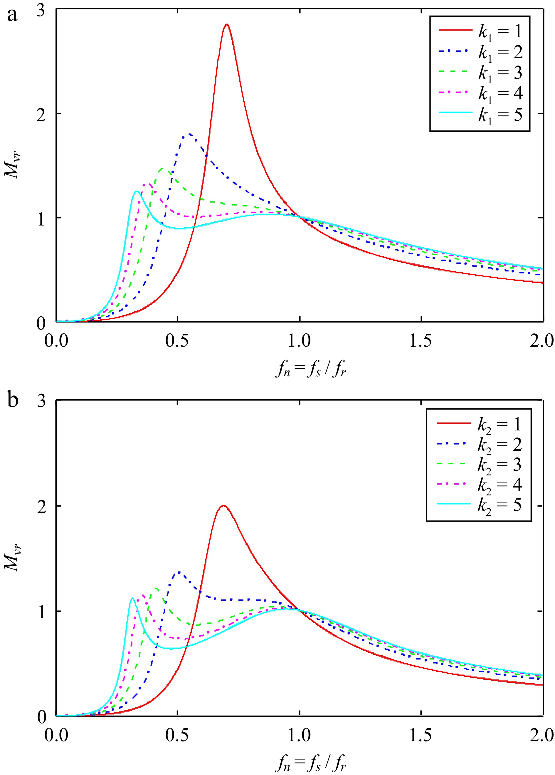
Figure 8.
(a) and (b) voltage gain curves for different k2 values in the charging and discharging mode. (a) Different k1 values in the charging mode. (b) Different k values in the discharging mode.
Dissipative coupling coil design simulation
-
This study combines the application of inductive coupling, because it adopts wireless transmission mode which is different from the traditional transformer. The winding shape of non-contact coupling transformer is shown in Fig. 9, in which the transmission coil and receiving coil are wound with multiple litz wires to reduce the skin effect caused by the high-frequency AC current, and a soft ferrite sheet is added under the coil, to increase the magnetic conductivity of the whole coil.
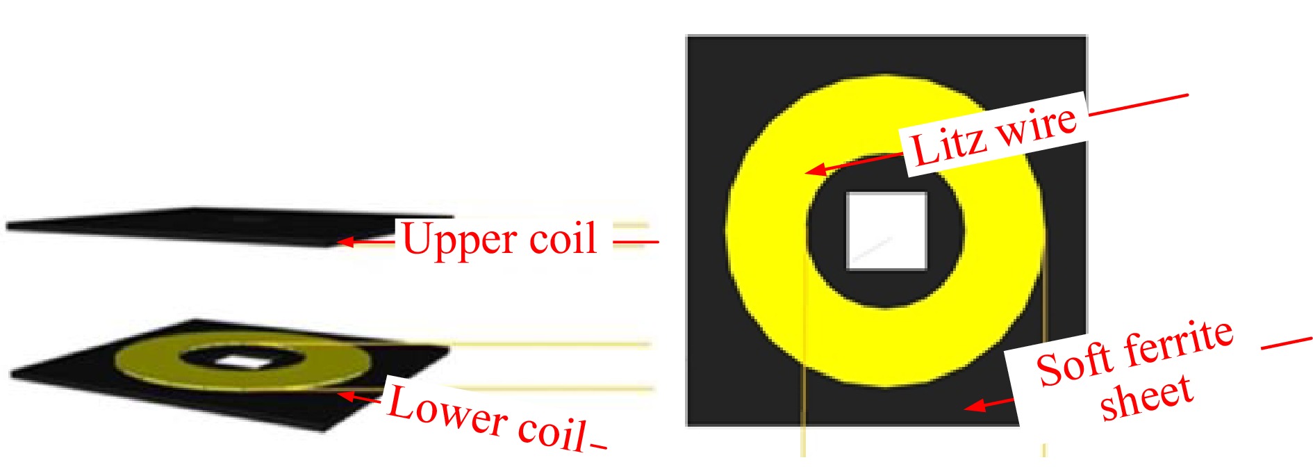
Figure 9.
Schematic of the coil disk.
When the coil is designed, the coupling coefficient and magnetic field line distribution will be greatly different due to different shapes of conductive coils and environmental effects, and the design is more complex. Therefore, through the simulation analysis software and the 2D/3D simulation software of low-frequency electromagnetic field, the finite element method (FEM) is used to simulate the accurate transient response of nonlinear electromagnetic field.
The following figures are simulated to verify whether the ferrite sheet can effectively improve the magnetic flux density. It is represented by color. Red is the highest magnetic flux density and blue is the lowest. Figure 10 is a wireless coil pair without a ferrite sheet for simulation. In the magnetic flux simulation of Fig. 11, it can be found that the magnetic flux distribution is relatively divergent.
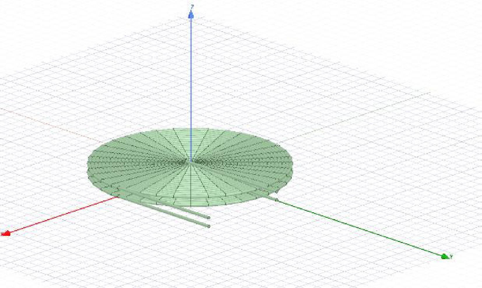
Figure 10.
Wireless coil pair without ferrite sheet.
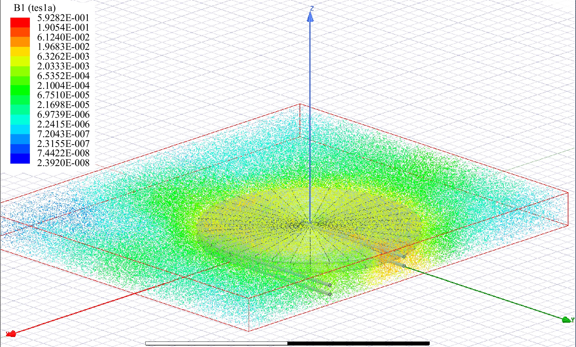
Figure 11.
Magnetic flux distribution of wireless coil pair without ferrite sheet.
Compared with the simulation analysis in the wireless coil of the ferrite sheet in Fig. 12, the magnetic flux can be concentrated on the coil pair through the ferrite sheet, which can improve the magnetic flux density to help transmit energy, as shown in Fig. 13.
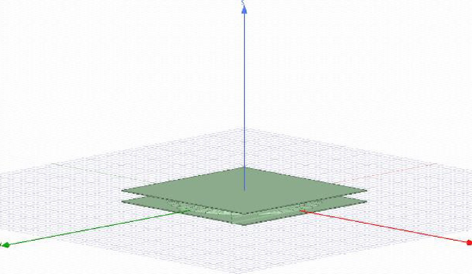
Figure 12.
Wireless coil pair with ferrite sheet.
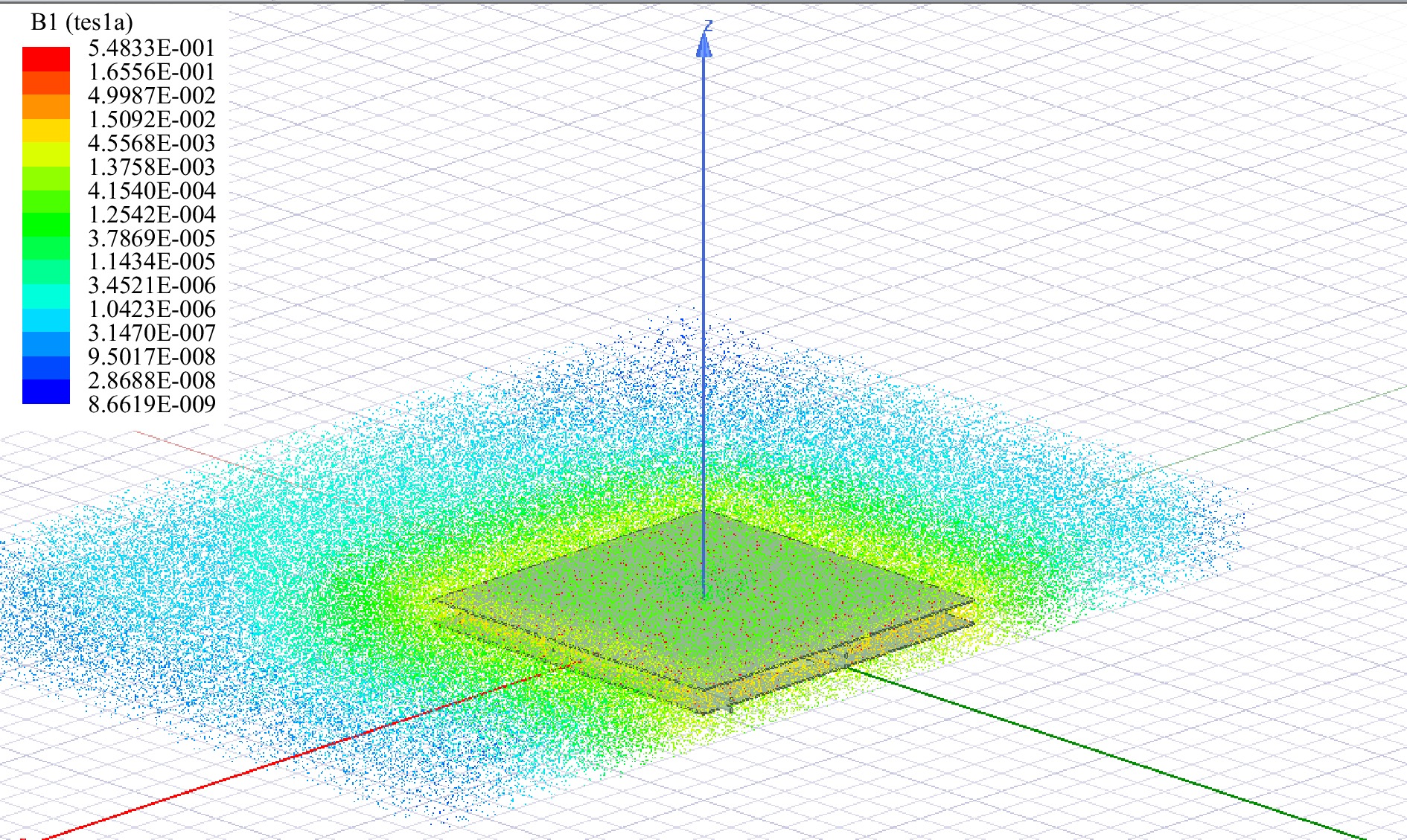
Figure 13.
Magnetic flux distribution of wireless coil pair with ferrite sheet.
-
In this study, the TMS320F28335 microprocessor developed by Texas Instruments was used to generate gate driver signals and monitor the input/output voltage and current of the proposed converter. Digital control has high information processing ability and multi-mode organization functions, such as ePWM module and A/D conversion module, which can process a large number of digital applications at the same time.
Figure 14 illustrates the digital control architecture of this study, where the A/D conversion module directly converts external analog voltage and current into digital signals for compensation purposes. Ultimately, the ePWM module generates a square wave with a frequency corresponding to the output signal to regulate the voltage and current power of the converter. No communication protocols were employed during the signal transmission process.
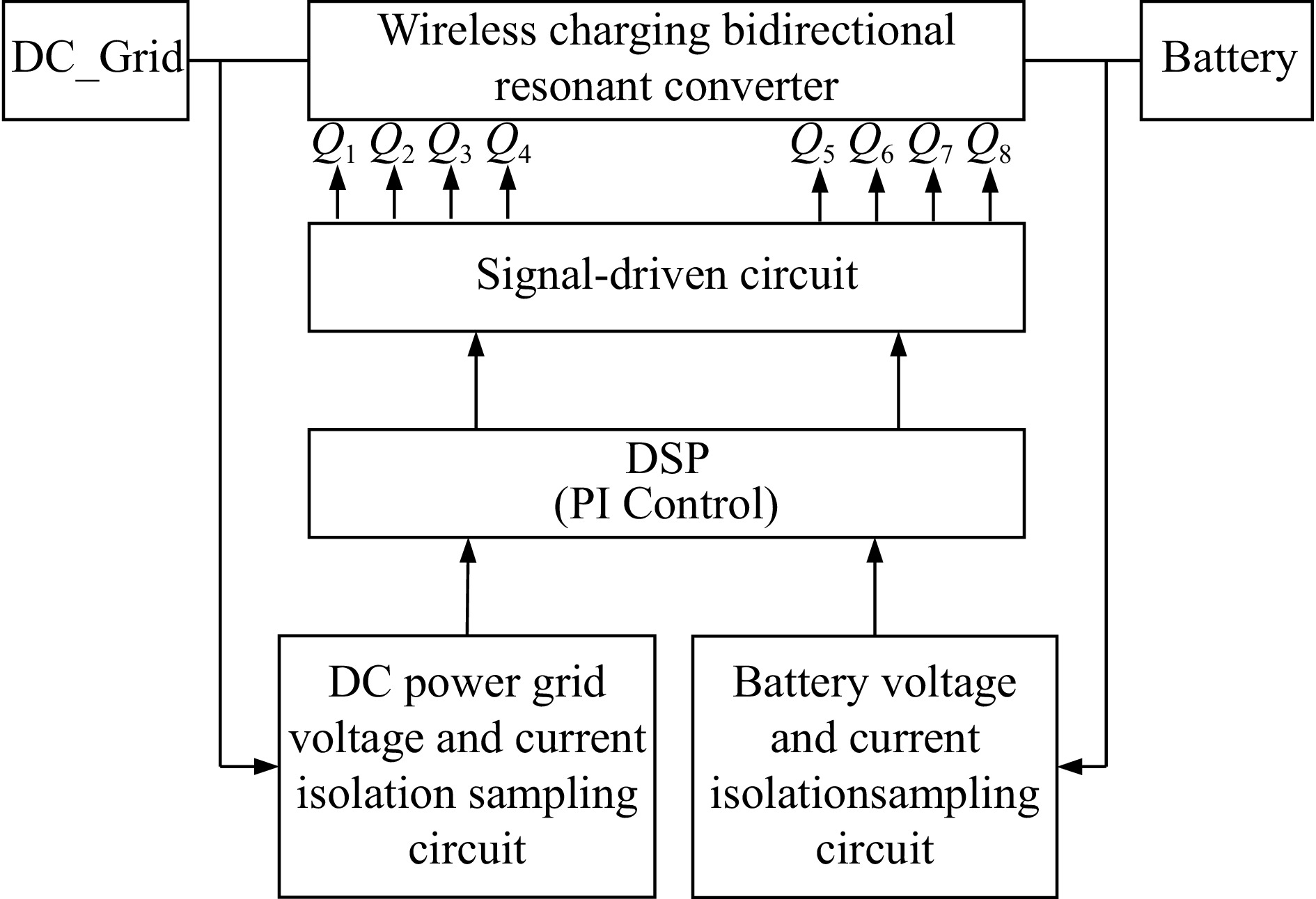
Figure 14.
Converter control architecture diagram.
When the converter operates in forward charging, the charging mode and its control method will be different. CC-CV combines the advantages of CV and CC to make the battery more stable during the charging process so that the battery does not age or damage easily. Figure 15 is a block diagram of a feedback system for charging a storage battery.
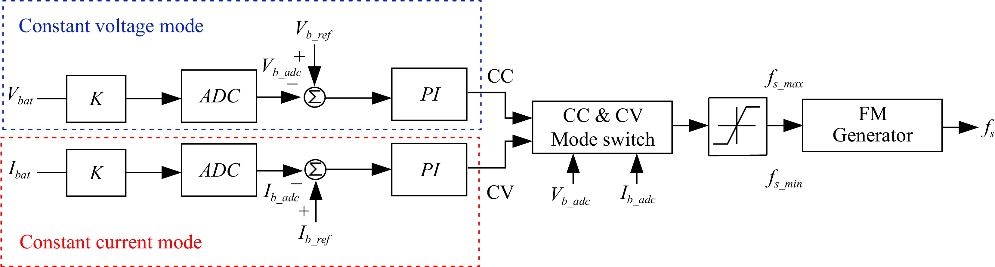
Figure 15.
Block diagram of positive charging storage and release battery terminal feedback system.
By detecting the battery charging voltage and current signal at the same time, the PI compensating circuit will determine CC or CV mode by programming algorithm, and finally generate a frequency-adjustable pulse signal through the FM waveform generator.
As shown in Fig. 16, the energy release feedback system block diagram is shown. To maintain a stable energy supply to the DC power grid, this mode of feedback uses CV mode.
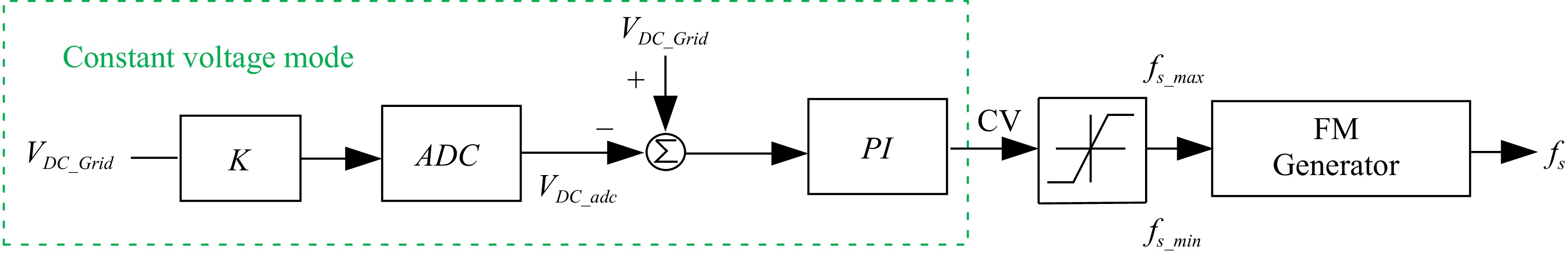
Figure 16.
Block diagram of DC grid end feedback system for reverse discharge.
During the design of the closed-loop system, the converter is affected by the control circuit, which makes it belong to a variable load. Therefore, it needs to be stabilized by the controller, which affects the response speed and safety of load change. Because the load varies continuously, the continuous-time function must be converted to the discrete-time function in the analysis. In this study, the proportional-integral (PI) control and the inverse Euler method are used for the control operation, as shown in Fig. 17.
$ Y\left(n\right)=Y\left(n-1\right)+{E}_{r}\left(n\right)\cdot {K}_{p}+{E}_{r}\left(n\right)\cdot {K}_{I}\cdot T $ (5) where, Kp: proportional gain; Ki: Integral gain; Er(n): Current error signal value; Y(n): Controller output value; Y(n-1): previous controller output value; T: System sampling frequency.
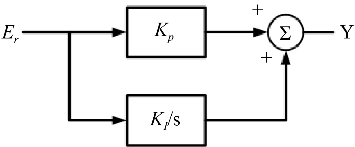
Figure 17.
PI controller block diagram.
In the design, the open-loop response of the converter is measured by the circuit analog software PSIM, and then the transfer function of the architecture is deduced by curve analysis by the mathematical operation software MATLAB. After the transfer function of the required PI compensator is calculated by the Control System Designer, the feasibility of the transfer function is verified by the analog circuit. Finally, the closed-loop control is implemented with the TMS320F28335 digital signal processor. In this study, the voltage-current mode is compensated by a single controller to achieve the function of definite voltage and current. For EV charging scenario, Table 1 shows the specification of the proposed EV charger in this study.
Table 1. The specification of the proposed EV charger.
Parameters Value DC grid voltage (VDC_Grid) 400 V Battery voltage (VBat) 280−400 V Maximum output current (IBat and Idc) 2.5 A Resonant frequency (fr) 100 kHz -
First, the required voltage gain is calculated based on the specifications for Charging Mode, accounting for a projected converter voltage drop loss of 10 V. To facilitate bidirectional energy transfer, the turns ratio N of the wireless coils is designed to be 1. The maximum and minimum voltage gains for forward charging can be expressed using Eqns (6) and (7).
$ {M}_{vr\text{}\_C\mathrm{}\_max}=\dfrac{N\cdot {V}_{Bat\text{}\_max}+{V}_{Loss}}{{V}_{DC\_Grid\mathrm{}}}=\dfrac{1\cdot 400+10}{400}\cong 1.03 $ (6) $ {M}_{vr\text{}\_C\_min}=\dfrac{N\cdot {V}_{Bat\text{}\_min}}{{V}_{DC\_Grid\mathrm{}}}=\dfrac{1\cdot 280+10}{400}\cong 0.73 $ (7) $ f_n=f_s\ /\ f_r $ (8) Based on the voltage gain formulas in Eqn (1) and the influence of various parameters on the voltage gain curve, it is necessary to satisfy the maximum and minimum gains for Charging Mode. Additionally, to simplify the feedback control, the curve is designed to exhibit a single peak characteristic. Since q1 is influenced by the load resistance, it is necessary to select curves that correspond to various loads while keeping parameters k1, g1, and h1 fixed. Therefore, the design standard is set to a maximum output load power of 400 V and 2.5 A. After iterative design, the parameters selected are k1 = 4.6, q1 = 0.3 (with VBat = 400 V and IBat = 2.5 A), g1 = 1, and h1 = 1, establishing the initial forward voltage gain curve for this circuit, as shown in Fig. 18.
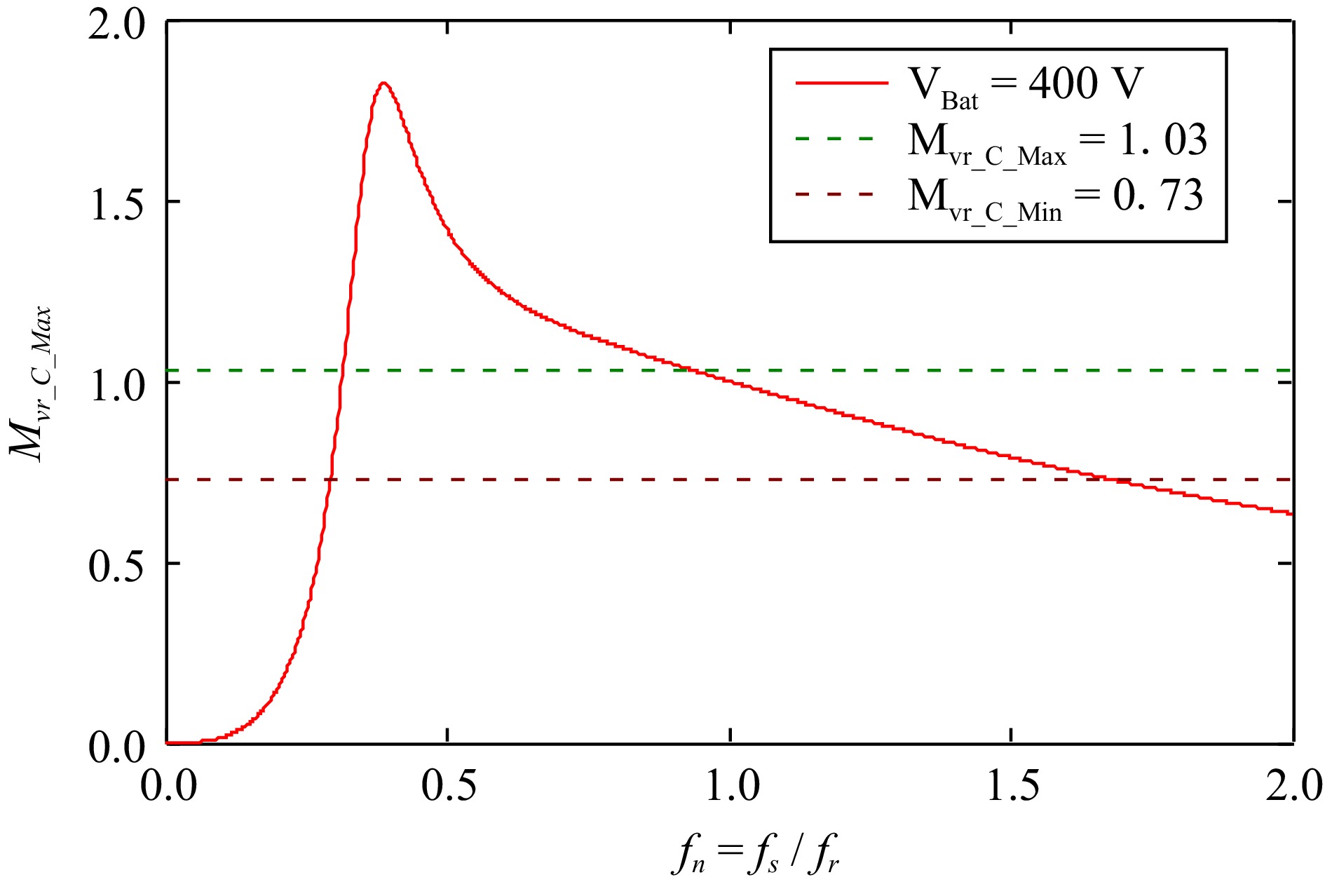
Figure 18.
Initial design of the charging mode gain curve.
Step 2. Derivation of charging mode resonance parameters
-
After determining the values of q1, k1, g1, and h1, the required resonant components for the wireless coils are derived using Eqns (3) and (9) through Eqn (12), as calculated in Eqns (13) to (16):
$ {R}_{eq}=\dfrac{{v}_{cd\text{},rms}}{{i}_{cd,rms}}=\dfrac{8}{{\pi }^{2}}{N}^{2}{R}_{Bat} $ (9) $ {L'_{r2}}={N}^{2}{L}_{r2} $ (10) $ {C'_{r2}}=\dfrac{1}{{N}^{2}}{C}_{r2} $ (11) $ {f}_{n1\_C}=\dfrac{{f}_{s}}{{f}_{r1}} $ (12) $ {R}_{oe\_400v}=\dfrac{8}{{\text π}^{2}}\cdot {N}^{2}\cdot \dfrac{{V}_{Bat}}{{I}_{Bat}}=\dfrac{8}{{\text π}^{2}}{\cdot 1}^{2}\cdot \dfrac{400}{2.5}\cong 129.7\Omega $ (13) $ {C}_{r1}=\dfrac{1}{2{\text π} \cdot {f}_{r{1}_{C}}\cdot {R}_{oe}\cdot {\mathrm{q}}_{1}}=\dfrac{1}{2{\text π} \cdot 100\mathrm{k}\cdot 129.7\cdot 0.299}\cong 41nF $ (14) $ {L}_{r1}=\dfrac{1}{{(2{\text π} \cdot {f}_{r1\_C})}^{2}\cdot {C}_{r1}}=\dfrac{1}{{(2{\text π} \cdot 100\mathrm{k})}^{2}\cdot 41n}\cong 61 \;{\text {μH}} $ (15) $ {L}_{m1}={L}_{r1}\cdot {k}_{1}=61{\text μ} \cdot 4.6\cong 280.6\;{\text {μH}} $ (16) Step 3: Wireless coil design and comparison with actual parameters
-
After the numerical comparison of simulated magnetizing inductance, shown in Table 2, it can be found that when the ferrite sheet is added, its magnetizing inductance is higher, which is conducive to reducing the winding area of the wireless coil.
Table 2. Comparison table of magnetic field simulation analysis data.
Without ferrite sheet Turns 10 20 30 Inductance 2.3 μH 6.1 μH 11 μH With ferrite sheet Turns 10 20 30 Inductance 50 μH 288.5 μH 700.6 μH According to the requirements of this study, the induction coil with 20 turns is wound and tested according to different air-gap distances, as shown in Table 3. Finally, it is proven by Eqn (17) that in the case of ferrite, when the coil distance changes, the mutual inductance M value also changes, affecting its conductivity.
Table 3. Test of changing coupling air-gap distance of wireless coil pair.
Air-gap distance (mm) Lm1 (μH) Lr1 (μH) Lm2 (μH) Lr2 (μH) 1 269.4 14 267.4 13.85 10 213.45 27.11 211.65 26.75 20 120.35 60.38 119.25 59.84 $ M=k\sqrt{{L}_{p}{L}_{s}} $ (17) Under the inductive coupling wireless transmission, most of them are resonant circuits, and the main control is PFM. Therefore, when the distance between the coils changes, the inductance ratio of the resonant inductance to the magnetizing inductance also varies accordingly. As indicated by Fig. 8, the change in the inductance ratio results in a steeper gain curve, making feedback control more difficult. Hence, this study adopts a fixed air-gap distance of 10 mm as the wireless energy transmission distance in this study. Also, considering the size and weight of the wireless coil pair, this study adopts 20 turns as the number of coils. The size of the coil is about 250 mm × 250 mm. Figure 19a shows the wireless coil pair with a ferrite sheet. The two coil discs are overlapped with each other to obtain the non-contact adjustable distance wireless coil pair, as shown in Fig. 19b.
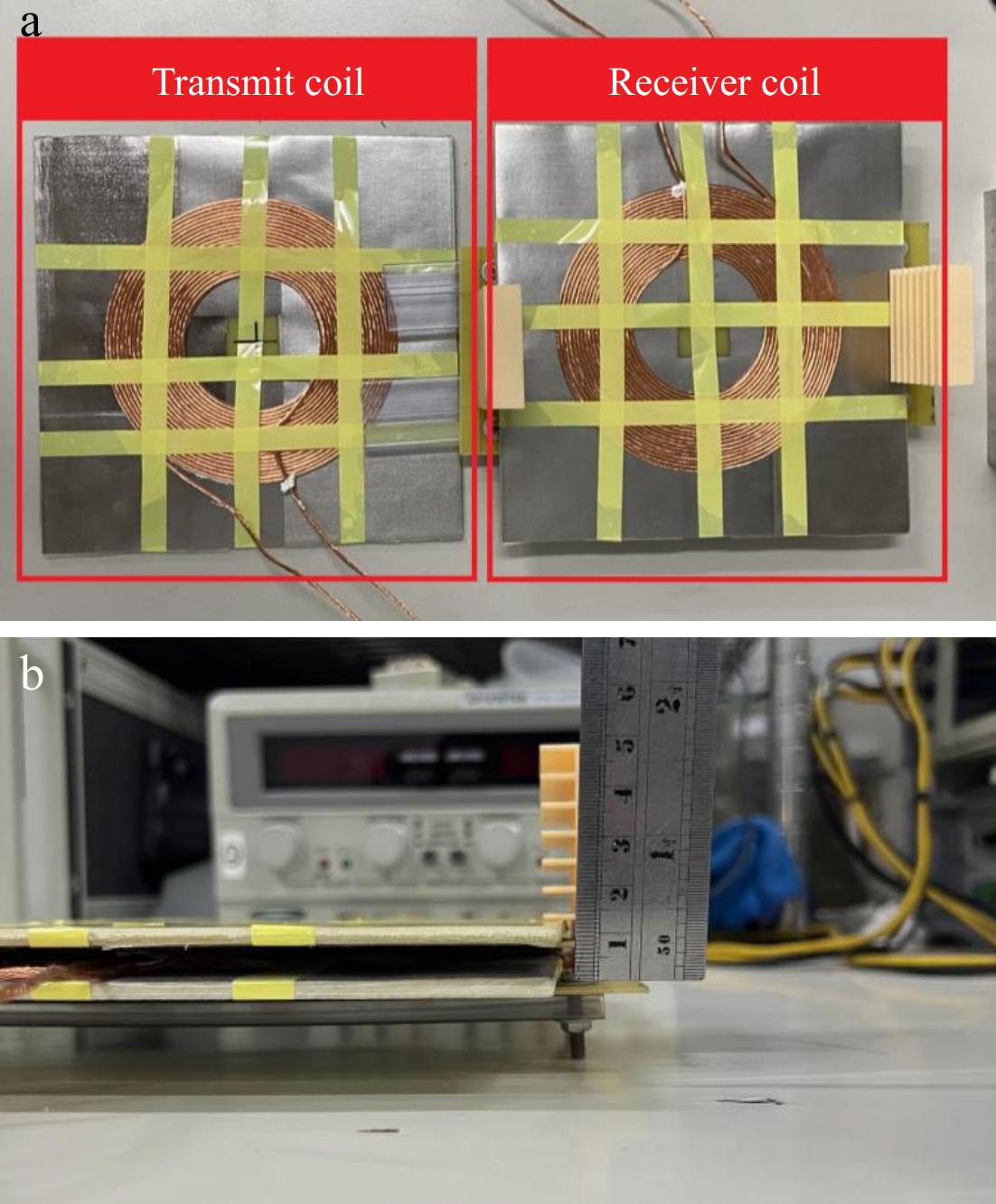
Figure 19.
Practical wireless coil pair. (a) Transmit coil and receiver coil. (b) Non-contact adjustable distance wireless coil pair.
Step 4. Corrected resonance parameters
-
After determining the inductance value of the wireless coil, the parameters differ from those in Step 1. Additionally, to align with the WPT design, the parameters for the wireless charging pad are reverse-engineered. With k1, g1, and h1 values held constant, the required resonant parameters for the wireless coil are derived from Eqns (3) and (9) through Eqn (12), as shown in Eqns (18) to (23). The design focuses on maximum voltage and full load output. As Lr1 and Cr1 vary, using Eqn (3), when VBat = 400 V and IBat = 2.5 A, q1 becomes 0.23. Considering an output voltage of VBat = 280 V with IBat = 2.5 A, the load resistance Roe changes, resulting in a q1 value of 0.33 for the second forward curve. The gain curves at different output voltages are illustrated in Fig. 20, all of which meet the required voltage gain.
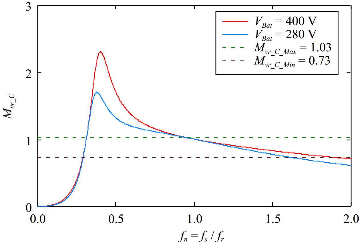
Figure 20.
The design of revised positive voltage gain curves.
$ {L}_{r1}=\dfrac{{L}_{m1}}{{k}_{1}}=\dfrac{213.45\mu }{4.6}\cong 46.4\mu H $ (18) $ {C}_{r1}=\dfrac{1}{{\left(2{\text π} \cdot {f}_{r{1}_{C}}\right)}^{2}\cdot {L}_{r1}}=\dfrac{1}{{\left(2{\text π} \cdot 100\mathrm{k}\right)}^{2}\cdot 46.4\mu }\cong 54nF $ (19) $ {L}_{r2}={L}_{r2}\cdot {\mathrm{N}}^{2}\cdot {h}_{1}\cong 46.4\mu H $ (20) $ {C}_{r2}=\dfrac{{L}_{r2}}{{\mathrm{N}}^{2}}\cdot {g}_{1}\cong 54nF $ (21) $ {q}_{1}=\dfrac{\sqrt{\dfrac{{L}_{r1}}{{C}_{r1}}}}{{R}_{oe\_400v}}=\dfrac{\sqrt{\dfrac{46.4\mu }{54n}}}{129.7}\cong 0.23 $ (22) $ {q}_{1}=\dfrac{\sqrt{\dfrac{{L}_{r1}}{{C}_{r1}}}}{{R}_{oe\_280v}}=\dfrac{\sqrt{\dfrac{46.4\mu }{54n}}}{90.8}\cong 0.33 $ (23) Step 5. Design of key circuit parameters k2, q2, g2, h2
-
Similar to the design steps in Step 1, the required voltage gain is calculated based on the specifications for DisCharging Mode. The maximum and minimum voltage gains for reverse discharge can be expressed using Eqns (24) and (25).
$ {M}_{vr\text{}\_\mathrm{D}\_max}=\dfrac{{V}_{DC\_Grid}+{V}_{Loss}}{N\cdot {V}_{\text{}Bat\mathrm{}\_min}}=\dfrac{400+10}{1\cdot 280}\cong 1.46 $ (24) $ {M}_{vr\text{}\_\mathrm{D}\_min}=\dfrac{{V}_{DC\_Grid}+{V}_{Loss}}{{N\cdot V}_{\text{}Bat\mathrm{}\_min}}=\dfrac{400+10}{1\cdot 400}\cong 1.03 $ (25) Using the mathematical expressions from Eqns (4) and (26) through Eqn (29), along with the component parameters derived from Eqns (18) to (23), a reverse numerical derivation is performed. Since this study employs a symmetrical structure, the parameters are all identical; however, for the sake of computation, they are referenced in Step 4 to derive Eqns (29) to (33).
$ {R'_{eq}}=\dfrac{{v}_{ab\text{},rms}}{{i}_{ab,rms}}=\dfrac{\dfrac{8}{{{\text π}}^{2}}{R}_{DC\_Grid}}{{N}^{2}} $ (26) $ {L'_{r1}}=\dfrac{1}{{N}^{2}}{L}_{r1} $ (27) $ {C'_{r1}}={{N}^{2}C}_{r1} $ (28) $ {R'_{oe}}=\dfrac{8}{{\text π}^{2}\cdot {N}^{2}}\cdot \dfrac{{V}_{DC\_Grid}}{{I}_{DC\_Grid}}=\dfrac{8}{{{\text π} }^{2}\cdot {1}^{2}}\cdot \dfrac{400}{2.5}\cong 129.7\Omega $ (29) $ {k}_{2}=\dfrac{\dfrac{{L}_{m1}}{{N}^{2}}}{{L}_{r2}}=\dfrac{\dfrac{213\mu }{{1}^{2}}}{47\mu H}\cong 4.6 $ (30) $ {q}_{2}=\dfrac{\sqrt{\dfrac{{L}_{r2}}{{C}_{r2}}}}{R'_{oe}}=\dfrac{\sqrt{\dfrac{46\mu }{54n}}}{129.7}\cong 0.23 $ (31) $ {g}_{2}=\dfrac{C'_{r1}}{{C}_{r2}}=\dfrac{{{N}^{2}\cdot C}_{r1}}{{C}_{r2}}\cong 1 $ (32) $ {h}_{2}=\dfrac{L'_{r1}}{{L}_{r2}}=\dfrac{{L}_{r1}}{{N}^{2}\cdot {L}_{r2}}\cong 1 $ (33) Finally, mathematical software is used to compute the DisCharging Mode voltage gain curve shown in Fig. 21. If the voltage gain does not meet the requirements, it will be necessary to return to Step 1 for redesign or to replace the wireless coil.
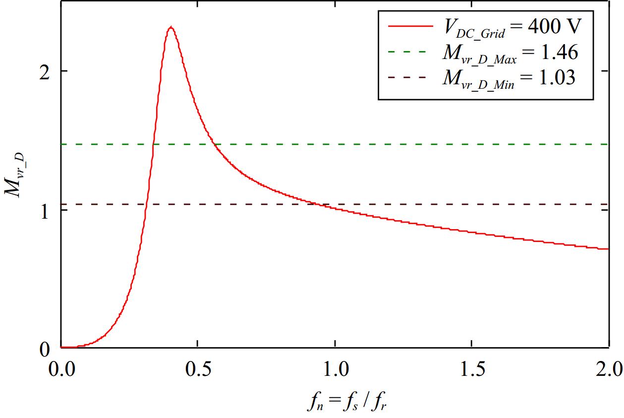
Figure 21.
Design of the discharging mode voltage gain curve.
-
Table 4 shows a 1 kW wireless power transfer symmetric resonant converter for bidirectional DC-DC circuits. The proposed converters are used between the DC grid and batteries to control two-way energy conversion for electric vehicles. The key circuit parameters of the components used in this converter are summarized in Table 4. The list of related experimental equipment and instruments is presented in Table 5.
Table 4. Key circuit parameters.
Parameters Value Transformer turns-ratio (Np : Ns) 1:1 Magnetizing inductance (Lm) 213.5 μH DC grid side resonant inductance (Lr1) 46.7 μH Battery side resonant inductance (Lr2) 46.1 μH DC grid side resonant capacitance (Cr1) 52 nF Battery side resonant capacitance (Cr2) 52 nF Filter capacitance (CDC_Grid) 540 μF Filter capacitance (CBat) 540 μF Power switches (Q1~Q8) UJ3C065080K3S Digital controller (Dsp) TMS320F28335 Table 5. Experimental and measurement instrumentation.
Instrument name Model DC power supply Chroma 62024P-600-8 Programmable DC electronic load Chroma 63202 Oscilloscope LeCroy HDO4034 Oscilloscope LeCroy 64Xi Voltage differential probes CYBERTEK DP6150A Current probes CYBERTEK CP8030A Power analyzer PM1000+ Battery recorders MIDI LOGGER GL800 Key waveforms for forward charging CV mode operation of the converter
-
This converter operates in forward charging CV mode with input voltage VDC_Grid is 400V, output voltage VBat is 400 V, output current is 0.25 to 2.5 A. Figure 22 show the vGS1, vDS1 and iDS1 waveforms of the power switch Q1. It can be seen from the waveforms that when the switch voltage vDS1 is 0 V, and the iDS1 current is in a countercurrent state. This current releases the parasitic capacitance stored energy on the power switch, causing the power switch Q1 to have zero overvoltage and the current to continue through the body diode of the power switch Q1, thus achieving the ZVS function.
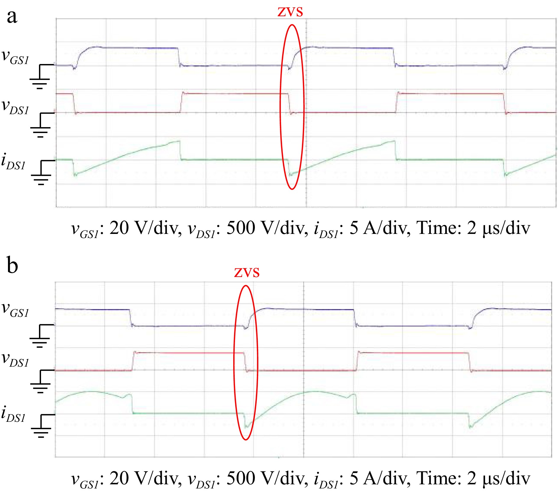
Figure 22.
Various waveforms of power switch Q1 with output current of (a) 0.5 A, and (b) 2.5 A in forward charging CV mode. (a) VDC_Grid = 400 V, VBat = 400 V, IBat = 0.5 A. (b) VDC_Grid = 400 V, VBat = 400 V, IBat = 2.5 A.
Figure 23 shows the input voltage vAB of the resonant tank and the input voltage vAB of the resonant current iLr1. It can be seen from the waveform that the square input voltage vAB of +VDC_Grid and −VDC_Grid is generated when the power switch on the controlled side interactively switches. When the output voltage VBat is 400 V, it can be seen that the resonant current iLr1 in the waveform is lagging the input voltage vAB. The resonant tank of the converter at this moment is inductive. Because the operation period 1/fs is larger than the resonance period 1/fr1, the resonant current is equal to the magnetizing current, and the wireless coupling coil pair enters the decoupling state. The resonant current increases linearly because of the influence of the magnetizing inductance. When the current on the rectifier side drops to zero ahead of time, the condition of ZCS can be reached.
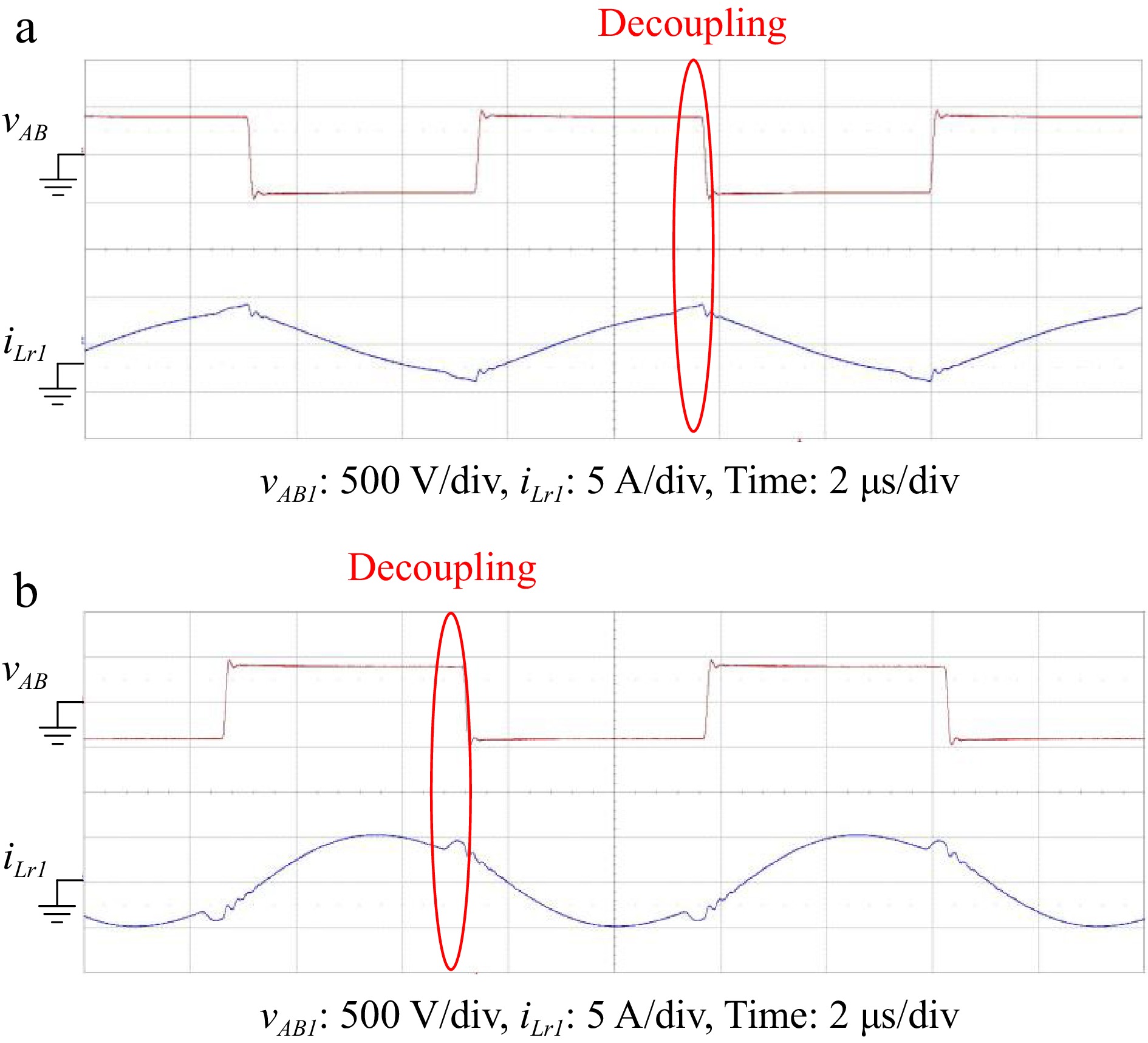
Figure 23.
Waveform of vAB and iLr1 under (a) 0.5 A, and (b) 2.5 A output current of forward charging CV mode. (a) VDC_Grid = 400 V, VBat = 400 V, IBat = 0.5 A. (b) VDC_Grid = 400 V, VBat = 400 V, IBat = 2.5 A
Key waveforms for forward charging CC mode operation of converter
-
This converter operates in forward charging CC mode with input voltage VDC_Grid is 400 V, output current IBat = 2.5 A, output minimum voltage 280 V and the maximum voltage 400 V. Figure 24a & b show the vGS1, vDS1, and iDS1 waveforms of the power switch Q1. It is known from the waveforms that ZVS is achieved on the switch. Since the output voltage 400 V is the same as CV mode, this is illustrated here with output 280 and 340 V.
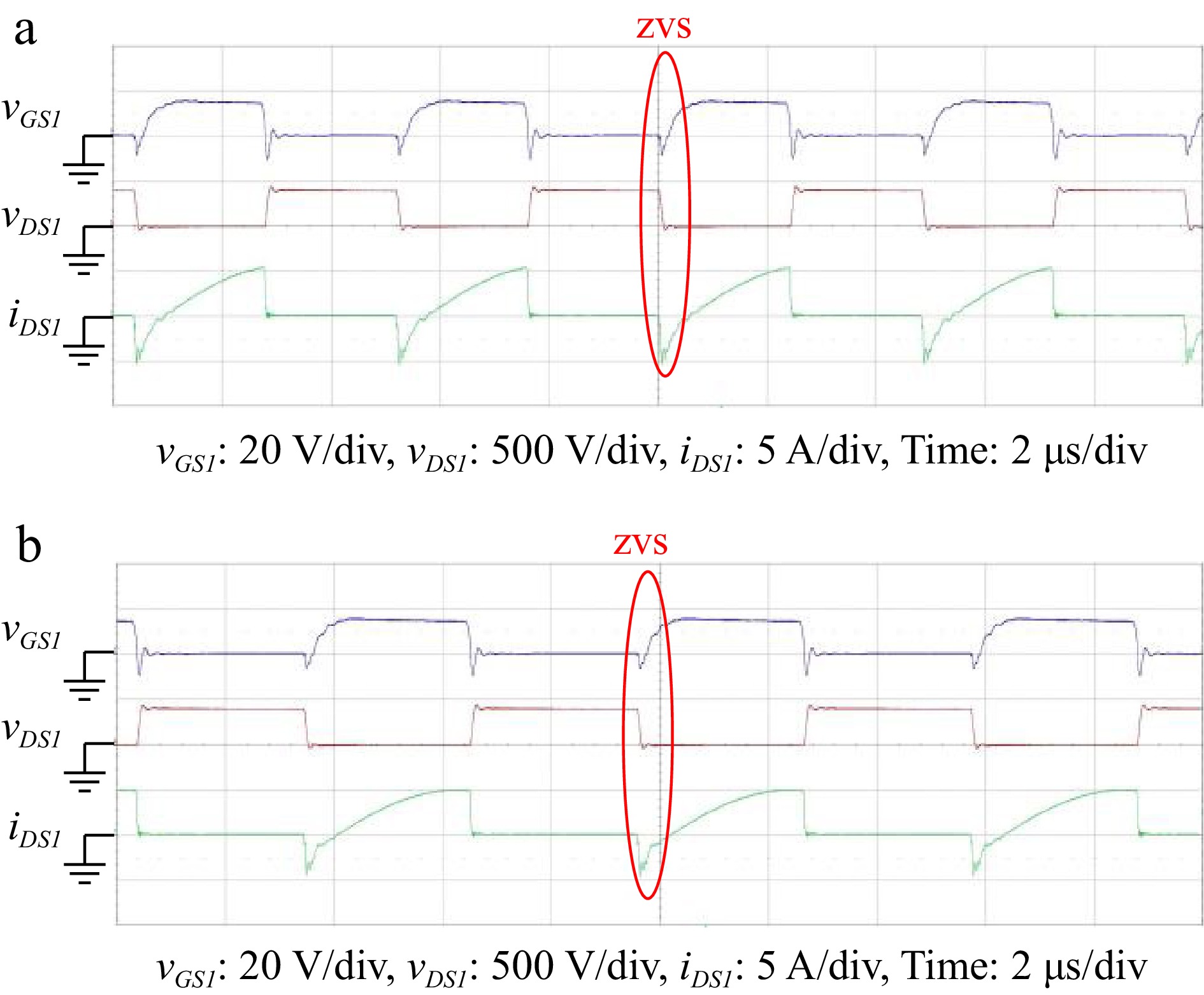
Figure 24.
Various waveforms of power switch Q1 with output voltage of 280 V and 340 V in forward charging CC mode. (a) VDC_Grid = 400 V, VBat = 280 V, IBat = 2.5 A. (b) VDC_Grid = 400 V, VBat = 340 V, IBat = 2.5 A
Figure 25 shows the waveforms of the input voltage vAB and the resonant current iLr1. It is known from the waveforms that the input voltage vAB of +VDC_Grid and –VDC_Grid. In CC mode, the output voltage is almost less than the resonant point voltage, and the operating period 1/fs is less than the resonant period 1/fr1. Therefore, no decoupling interval is generated and ZCS is not achieved on the rectifier side.
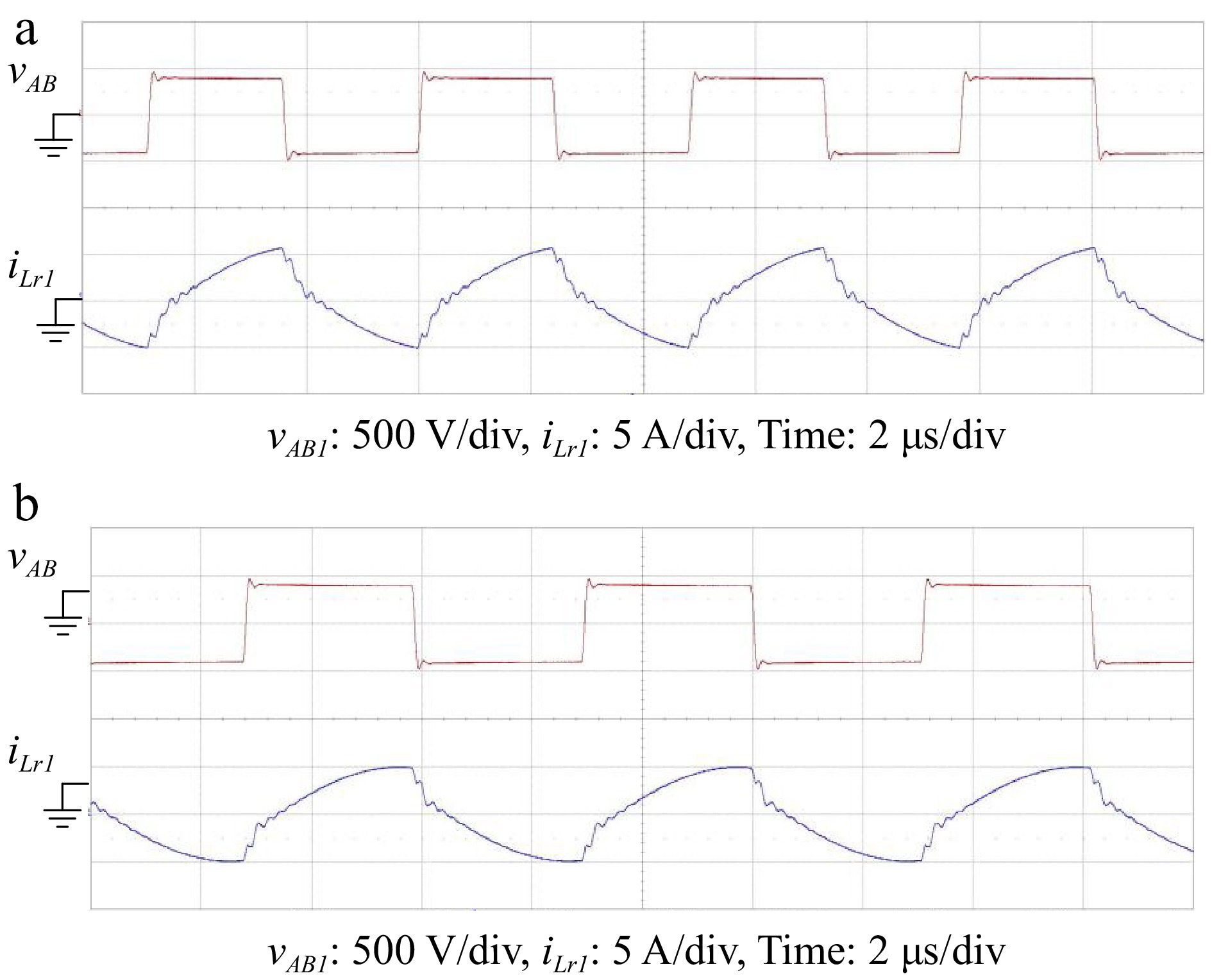
Figure 25.
Waveform of vAB and iLr1 under 280 V, and 340 V output voltage of forward charging CC mode. (a) VDC_Grid = 400 V, VBat = 280 V, IBat = 2.5 A. (b) VDC_Grid = 400 V, VBat = 340 V, IBat = 2.5 A.
After testing in CV mode, the efficiency curve of CV charging is plotted for each load from 100 W to 1 kW. According to Fig. 26, it can be concluded that the transmission loss of the wireless coil pair affects the conversion efficiency of the light load condition, but with the increase of the load, the transmission loss caused by the wireless coil does not increase significantly, so the full load efficiency can be improved and is up to 89.25%.
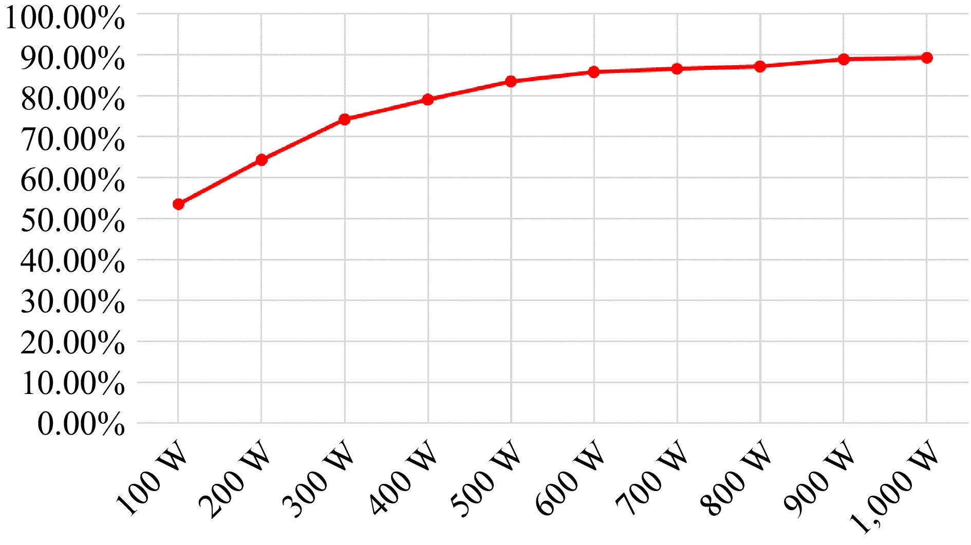
Figure 26.
Efficiency curve for forward charging CV mode.
The following efficiency curve is measured for CC mode and the efficiency curve is obtained with a constant current of 2.5 A for step rising voltage variation from 280 to 400 V, the maximum efficiency can reach 90.19% at 380 V which is shown in Fig. 27.
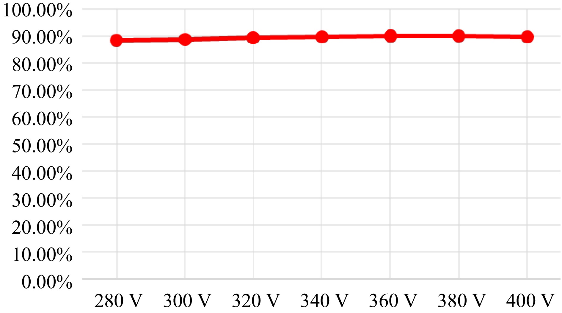
Figure 27.
Efficiency curves for forward charging CC mode with varying output voltage.
Key waveforms for reverse discharging operation of converter
-
The converter operates in reverse discharging mode. The input voltage Vbat range is from 280 to 400 V, while the output voltage and output current are 400 V and 2.5 A respectively. As shown in Fig. 28, the vGS5, vDS5, and iDS5 waveforms of power switch Q5 can be seen from the waveforms. When the vDS5 is reducing to 0, the iDS5 current presents a countercurrent state. This current releases the stored energy of the parasitic capacitor on the power switch so that the cross voltage on power switch Q5 is zero, and the current continues to flow through the intrinsic diode. At this time, ZVS is achieved.
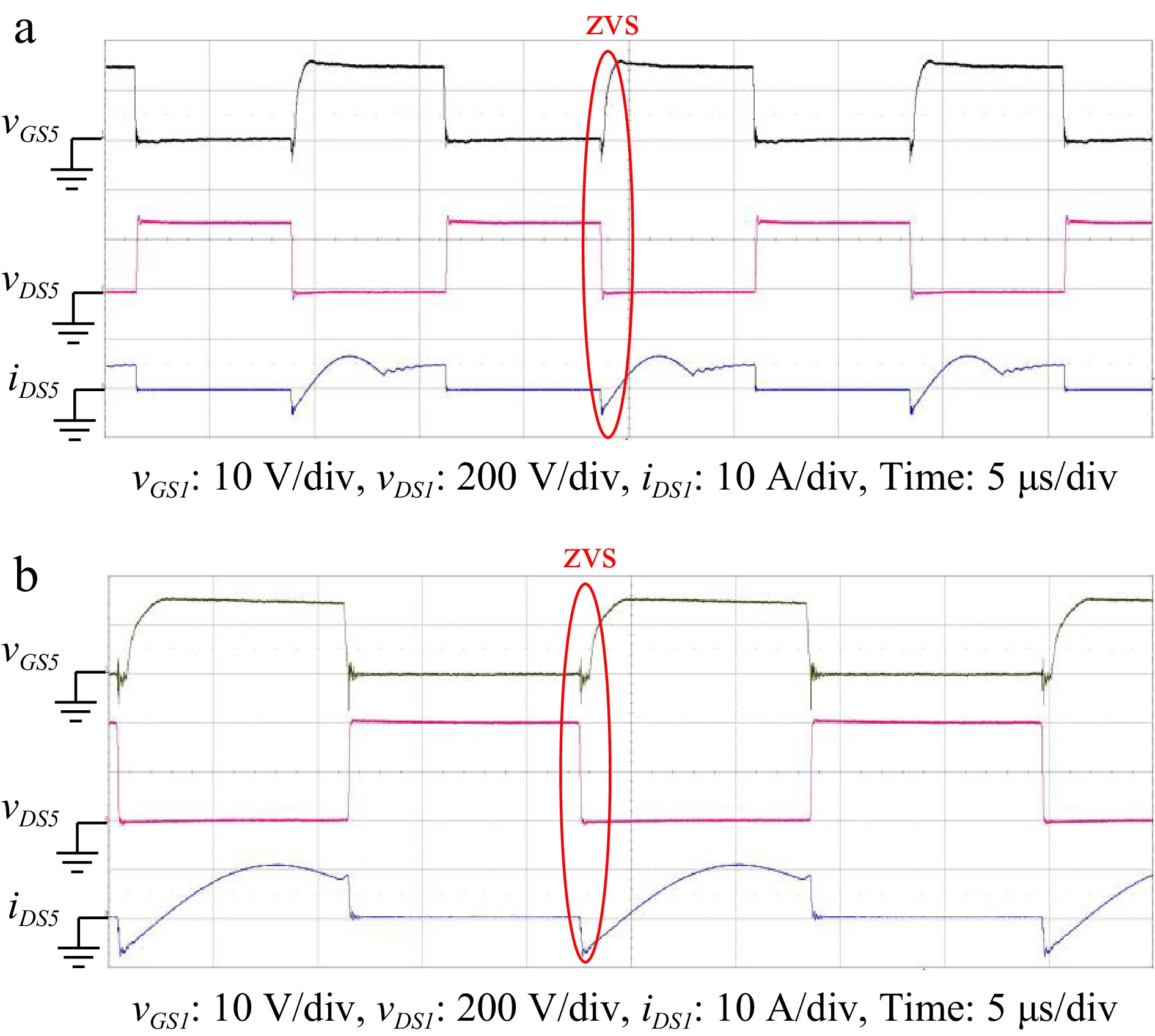
Figure 28.
Various waveforms of power switch Q5 with input voltage of (a) 280 V, and (b) 400 V in reverse discharging. (a) VBat = 280 V, VDC_Grid = 400 V, IBat = 2.5 A. (b) VBat = 400 V, VDC_Grid = 400 V, IBat = 2.5 A.
Figure 29 shows the waveforms of the input voltage vCD in front of the resonant slot and the resonant current iLr2. It can be seen from the waveforms that the input voltage vCD of +VBat and –VBat is generated. When the output voltage VDC_Grid = 400 V, due to the operation cycle 1/fs is longer than the resonant cycle 1/fr2 and the resonant current equals the magnetizing current. When the wireless coil pair enters the decoupling region, the resonant current increases linearly. The rectifier current is zero; hence the ZCS is achieved.
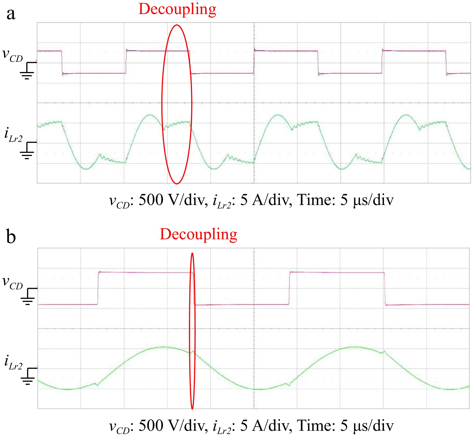
Figure 29.
Waveform of vCD and iLr2 under (a) 280 V, and (b) 400 V battery voltage of reverse discharging. (a) VBat = 280 V, VDC_Grid = 400 V, IBat = 2.5 A. (b) VBat = 400 V, VDC_Grid = 400 V, IBat = 2.5 A.
The efficiency curves with detailed measurement data of three different constant output voltage under load variation are drawn in Fig. 30. When the minimum voltage is 280 V, the maximum efficiency is 90.03%. The intermediate voltage is 340 V, and the maximum efficiency is 89.29%. When the maximum voltage is 400 V, the maximum efficiency is 89.64%.
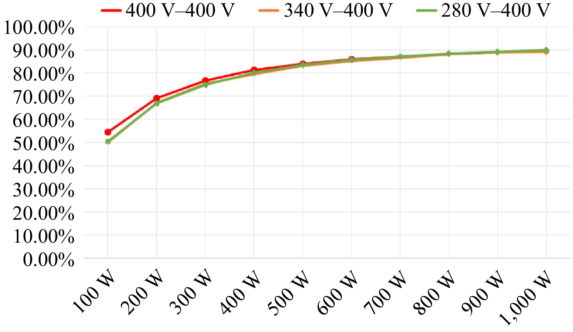
Figure 30.
Efficiency curve of each load under different input voltage in reverse discharging mode.
Practical battery charging experiment and verification
-
In this section, a ANR26650m1b lithium iron phosphate battery (LiFePO4) is used as the energy storage and release device. The designed voltage and capacity will be achieved in series and parallel connections. The specification is shown in Table 6. The converter will achieve the voltage, current detection, and switching function of the charger through digital control. Finally, the practical battery charging process is verified by recording the charging voltage curve, current curve, and the charging time.
Table 6. Battery specifications.
Parameters Value Lowest voltage 280 V Standard voltage 369.6 V Recommend charging voltage 400 V Capacity 5.2 Ah Impedance 336 mΩ Energy 1.85 kWh As shown in Fig. 31, the initial battery voltage is about 288 V. When charging starts, the converter is operated for constant current (CC) mode with a stable 2.5 A output current as shown in red. At this time, according to the battery chemical reaction, the battery voltage rises to the standard voltage and continues to charge. When the battery's voltage reaches 400 V, the battery's energy is almost full, the converter changes to constant voltage (CV) charging mode. The chemical reaction of the battery slows down, but this CV charging mode can make the battery charge to full energy slowly and reduce the impact of charging loss. The CC mode charging time is about 1.83 h, and the CV mode time is about 0.33 h. According to the datasheet of ANR26650m1b, it is suitable for 0.5 c charging current. Therefore, the total charging time is about 2.2 h. It is confirmed and verified that the proposed converter can achieve the function of CC-CV charging mode of the practical battery charging process.
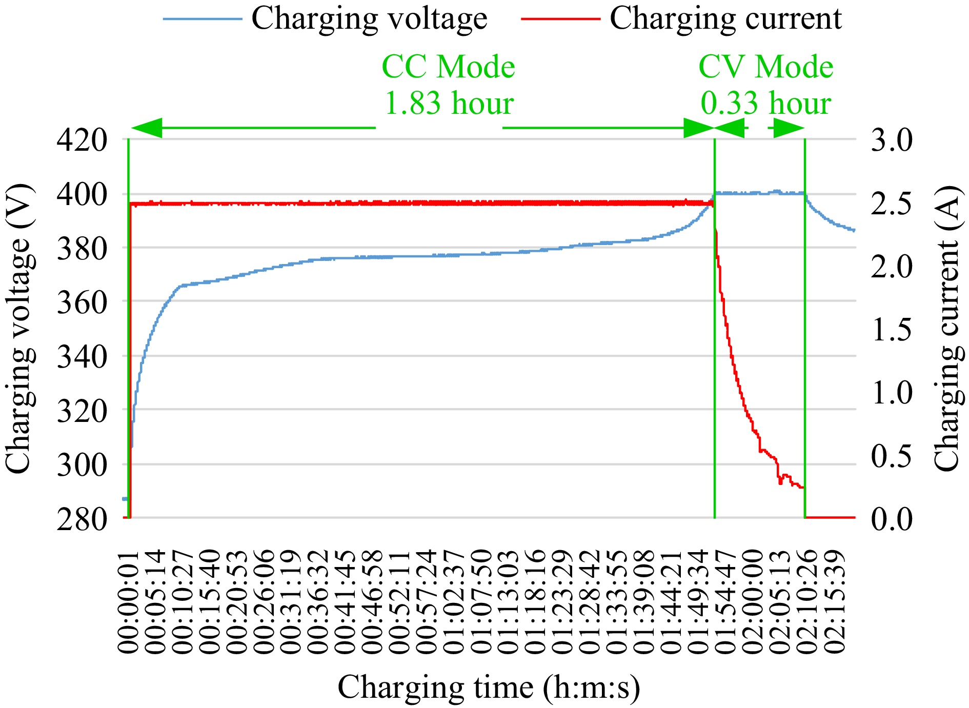
Figure 31.
CC-CV charging voltage-current curve.
When the circuit starts, since the output voltage is below the charging upper limit of 400 V, the converter operates in CC mode with a fixed current of approximately 2.5 A, and the output voltage continues to rise. When the voltage reaches 400 V, the converter switches to CV mode, at which point the output voltage is fixed. The battery voltage continues to rise, causing the voltage difference to decrease and the current to gradually drop until the battery is fully charged. This mechanism reduces the chemical reaction as the battery nears full charge, minimizing wear, and extending the battery's lifespan. As illustrated in Fig. 32, the waveforms simulate the transition of battery charging from CC mode to CV mode.
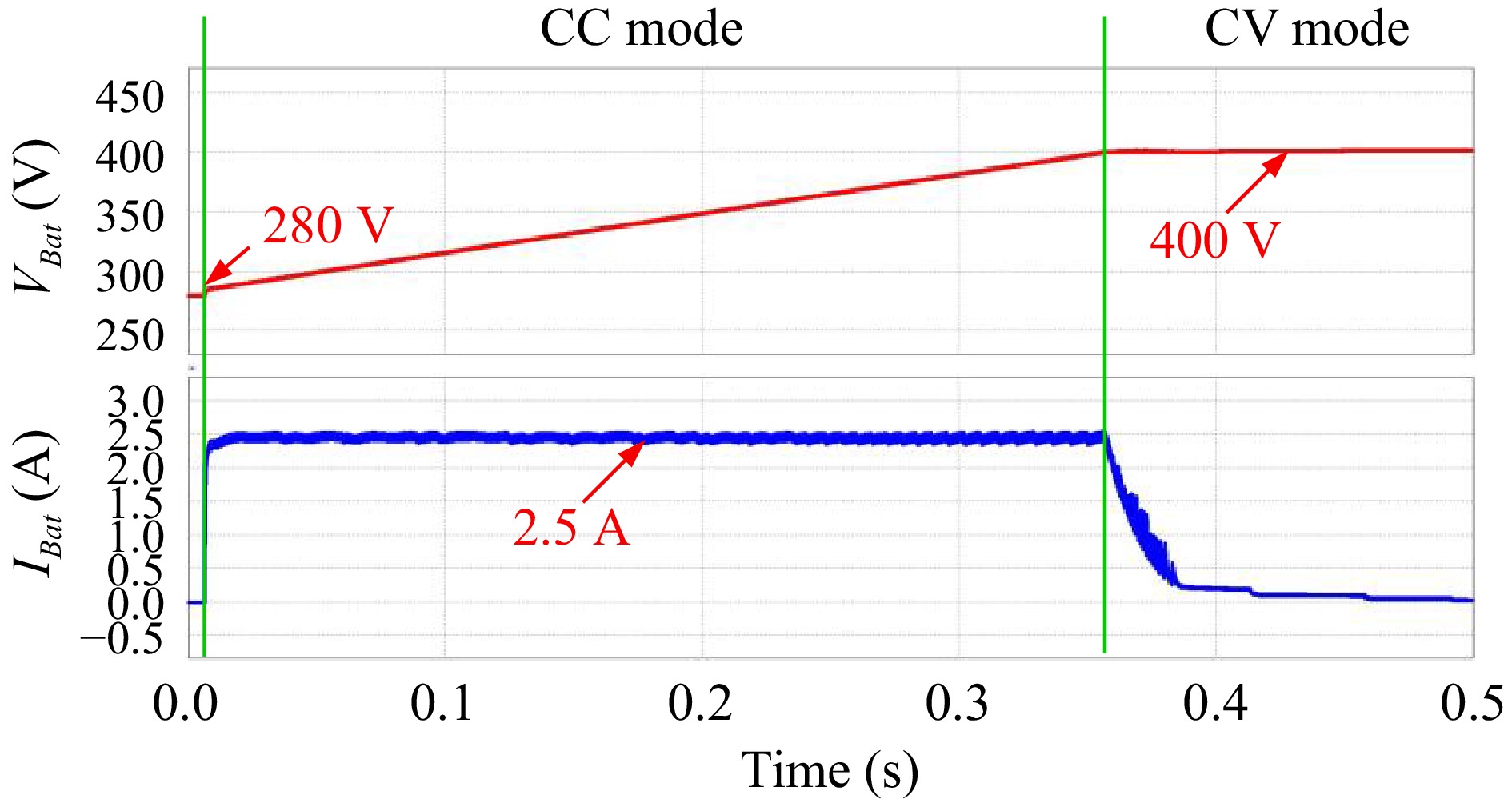
Figure 32.
CC-CV charging state simulation.
-
A wireless bidirectional symmetrical resonant converter with wide-range regulation of input and output voltage is implemented. In this proposed converter, a resonant element is added to the secondary side of the traditional LLC resonant converter, and the rectifier diodes are replaced by the body diodes of power switches to achieve the dual active full bridge power switching architecture. Hence, the circuit can be utilized for the application of bidirectional energy transfer. Under wide load output, the power switches have soft switching characteristics, it improves the overall converter efficiency and wide output functions. In this study, the bidirectional power conversion and wireless power transmission of power grid terminal 400 V and battery terminal voltage 280 to 400 V are completed. The experimental results show that the maximum efficiency of the converter can reach 90.19% in the forward charging mode and 90.03% in the reverse power transmission mode. Finally, the proposed converter with CC-CV charging mode is also implemented and verified to achieve the constant current and constant voltage charging strategies.
This work was supported by the National Science and Technology Council, project number NSTC 110-2221-E-150-017.
-
The authors confirm contribution to the study as follows: study conception and design: Wu ST; data collection: Chen JY; analysis and interpretation of results: Wu ST, Chen JY; draft manuscript preparation: Wu ST. Both authors reviewed the results and approved the final version of the manuscript.
-
The datasets generated during and/or analyzed during the current study are available from the corresponding author on reasonable request.
-
The authors declare that they have no conflict of interest.
- Copyright: © 2025 by the author(s). Published by Maximum Academic Press, Fayetteville, GA. This article is an open access article distributed under Creative Commons Attribution License (CC BY 4.0), visit https://creativecommons.org/licenses/by/4.0/.
-
About this article
Cite this article
Wu ST, Chen JY. 2025. Implementation of a CC-CV wireless charging bidirectional resonant converter for electric vehicles. Wireless Power Transfer 12: e002 doi: 10.48130/wpt-0024-0014 

Implementation of a CC-CV wireless charging bidirectional resonant converter for electric vehicles
- Received: 22 August 2024
- Revised: 28 October 2024
- Accepted: 31 October 2024
- Published online: 24 January 2025
Abstract: In this study, a contactless bidirectional power converter with magnetic induction is proposed to transfer the power bi-directionally between a DC power grid and EV battery with a digital control mechanism. In this study, the dual active full bridge is used as the energy conversion structure. The proposed symmetrical resonant topology has the following features. It can achieve a wide input and output voltage range, reduce the complexity of bidirectional circuit design, and make the converter with soft switching characteristics for reducing circuit losses. The proposed scheme with wireless energy transmission technology to transfer energy through the air gap. Besides, digital control is used to stabilize the current and the voltage for CC and CV charging requirement. Finally, the theoretical analysis is verified to achieve a 400 V DC power grid and 280−400 V battery voltage, and the two-way maximum efficiency is 90.19%. The actual charging test of the storage and release battery is carried out to verify that the control of this study can reach the CC-CV charging method.