-
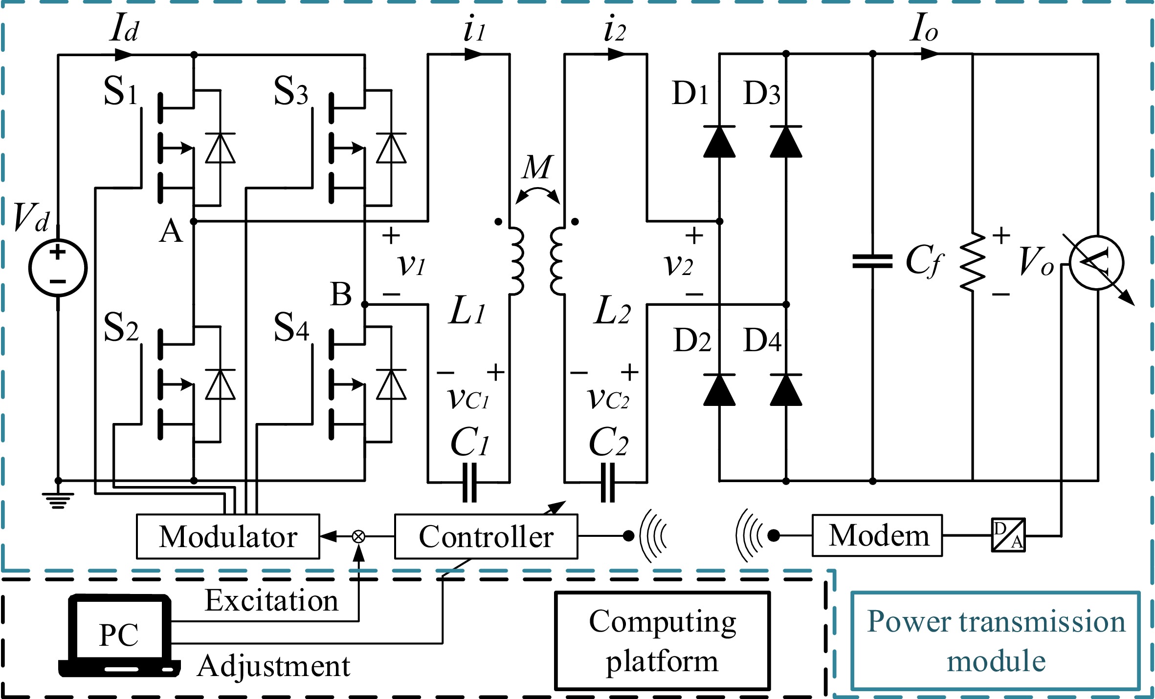
Figure 1.
The topology of the WPT system.
-
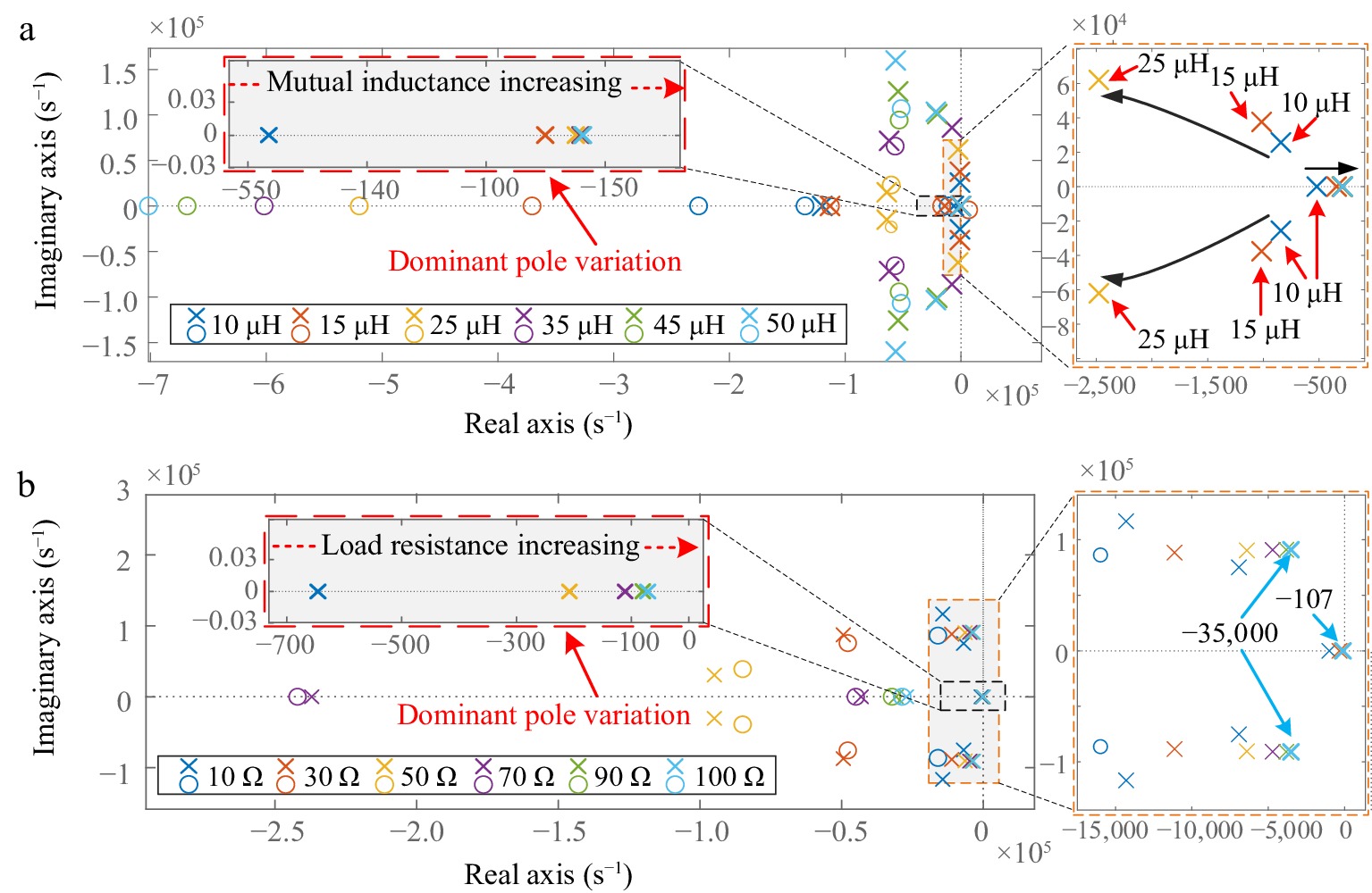
Figure 2.
Zero-pole distribution plot. (a) Zero-pole distribution under mutual inductance. (b) Zero-pole distribution under load resistance variation.
-
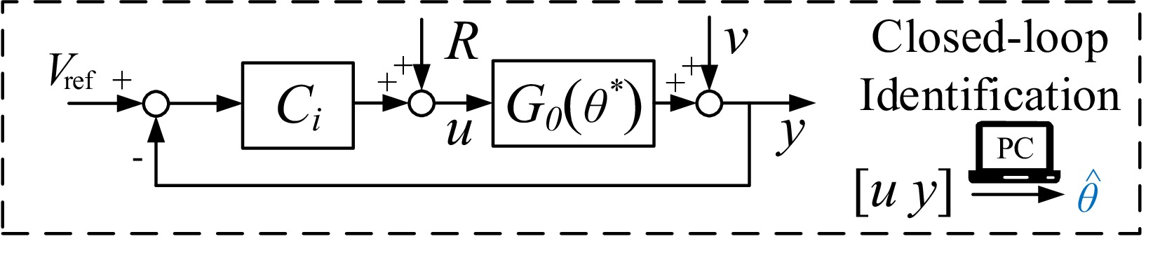
Figure 3.
Identification scheme diagram.
-
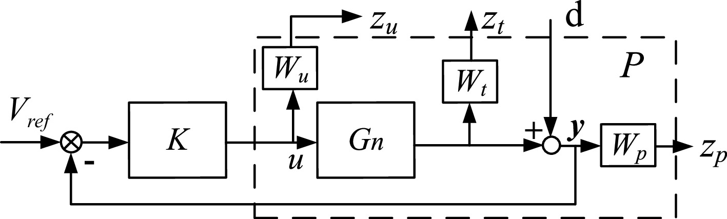
Figure 4.
Structure diagram of H∞ problem for the WPT system.
-
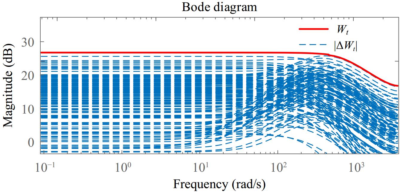
Figure 5.
Structure diagram of H∞ problem for the WPT system.
-
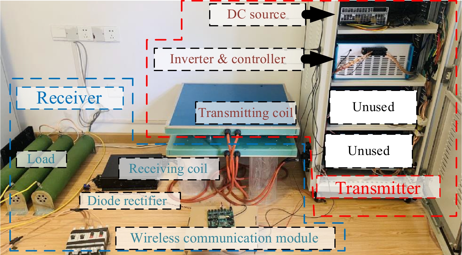
Figure 6.
Circuit topology for the WPT system under consideration.
-
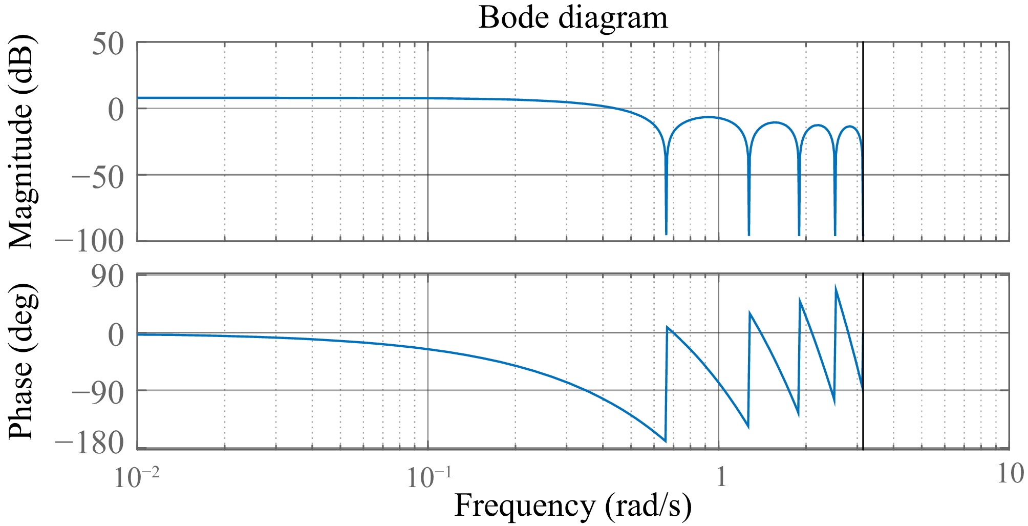
Figure 7.
Bode plot of the optimal spectrum H.
-
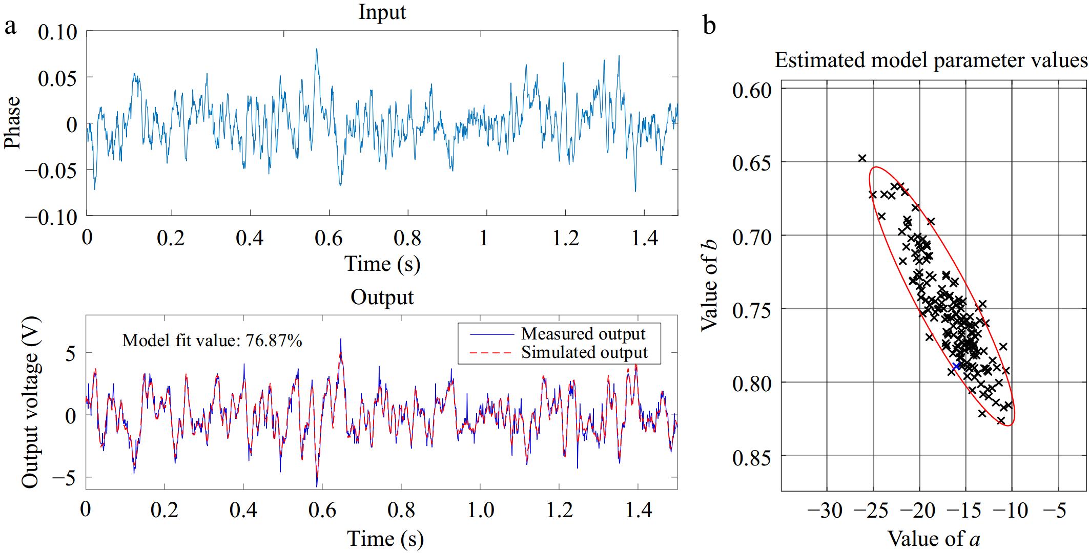
Figure 8.
Identification results. (a) Portion of input and output generated from the LMI optimization excitation signal. (b) The estimated model parameter values.
-
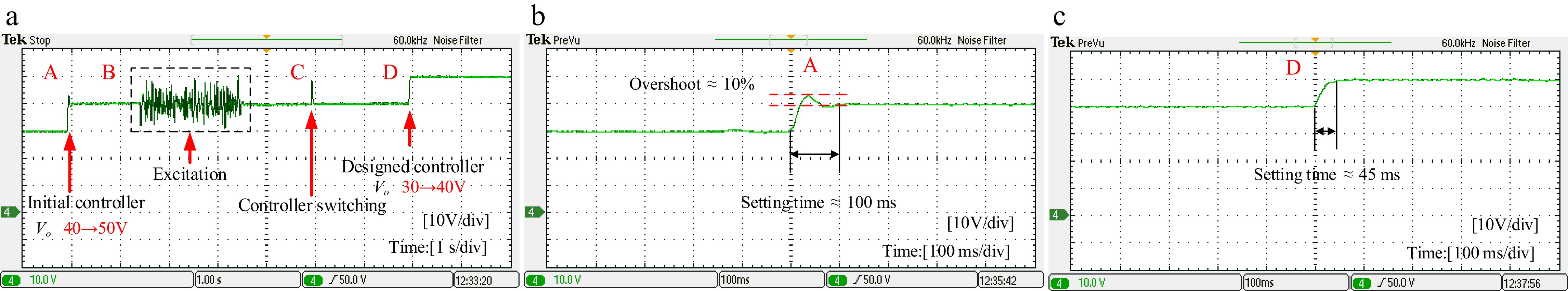
Figure 9.
Voltage variation control experiment based on system identification. (a) Overall view of voltage step response, system excitation, and controller switching. (b) V0 increase from 30 to 40 V. (c) V0 increase from 40 to 50 V.
-
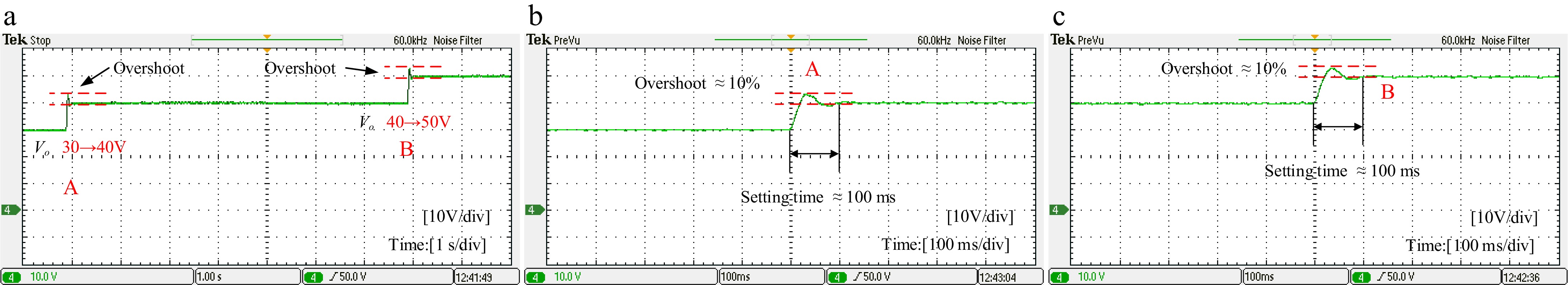
Figure 10.
Voltage variation control experiment with constant controller. (a) Overall view of voltage step response. (b) V0 increase from 30 to 40 V. (c) Vo increase from 40 to 50 V.
-
Parameters Values Switching frequency f0 92 kHz DC voltage VD 50 V Self-inductance of primary coil L1 117 μH Self-inductance of secondary coil L2 116 μH Primary resonant capacitance C1 26 nF Secondary resonant capacitance C2 25.4 nF Mutual inductance M 37 μH Filter capacitance Cf 450 μF Load resistance RL 35 Ω Sampling time Ts 1 ms Table 1.
System design parameters.
-
Proposed method White noise PRBS Output power (w) 0.40 0.40 0.41 Fit value (%) 76.87 55.19 68.04 Table 2.
Comparison of various typical signals.
Figures
(10)
Tables
(2)