-
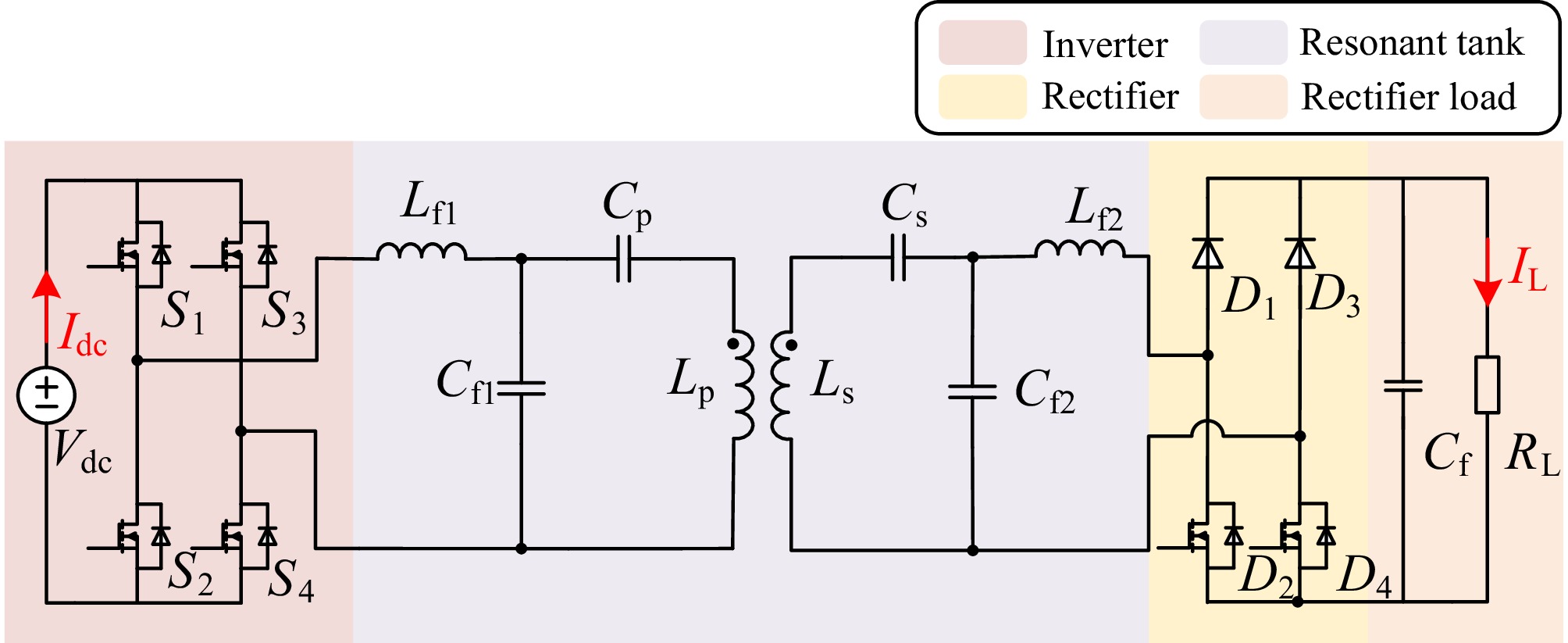
Figure 1.
Dual-side LCC WPT system with an active rectifier.
-
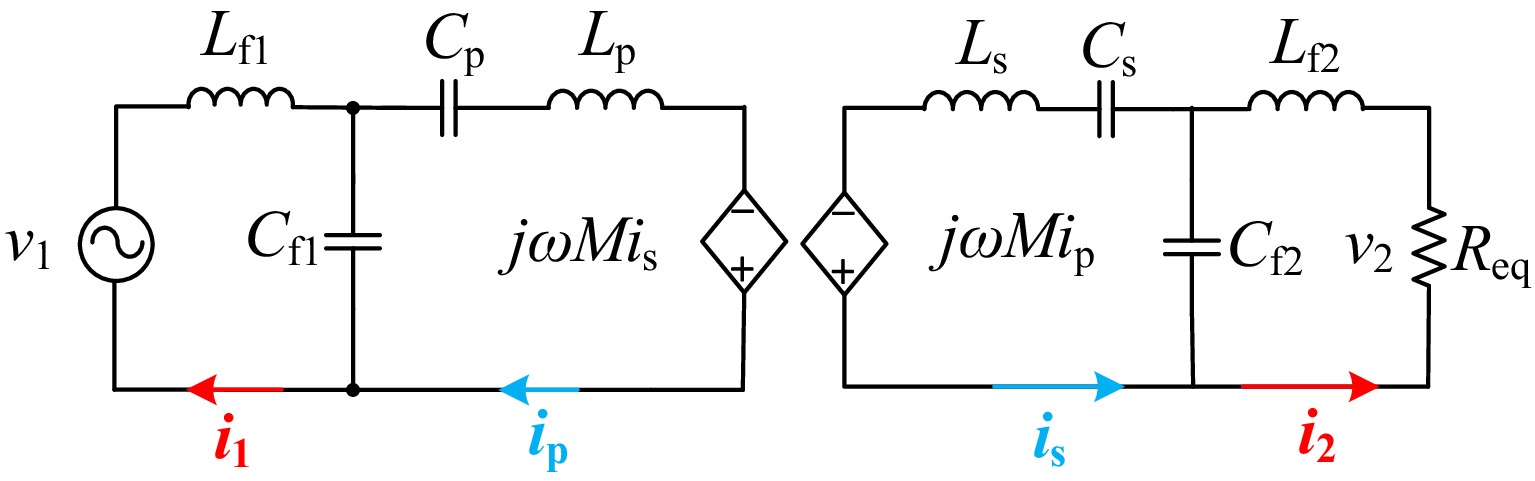
Figure 2.
Equivalent circuit of the dual-side LCC WPT system.
-
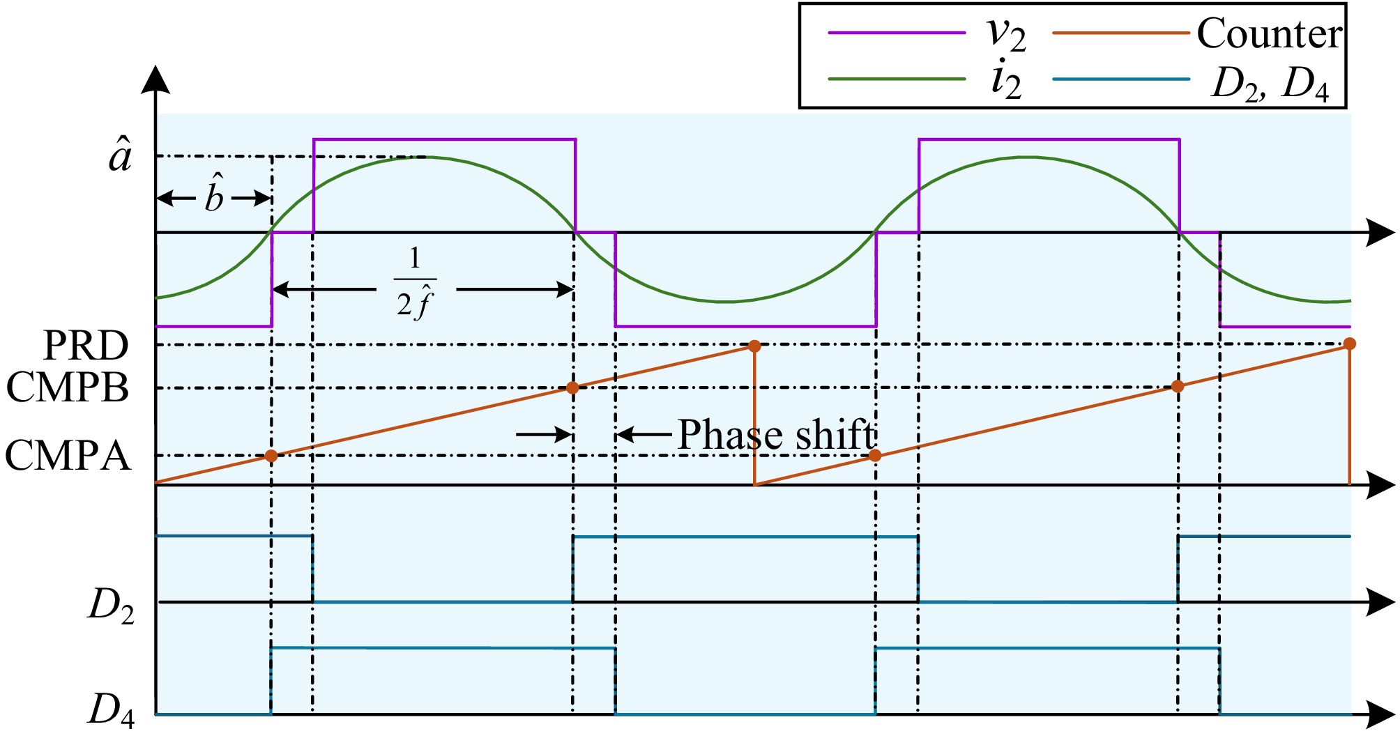
Figure 3.
Generation of the driving signals for D2 and D4. PRD is the period of the PWM counter, CMPA is the counter value to switch on D4, and CMPB is the counter value to switch on D2.
-
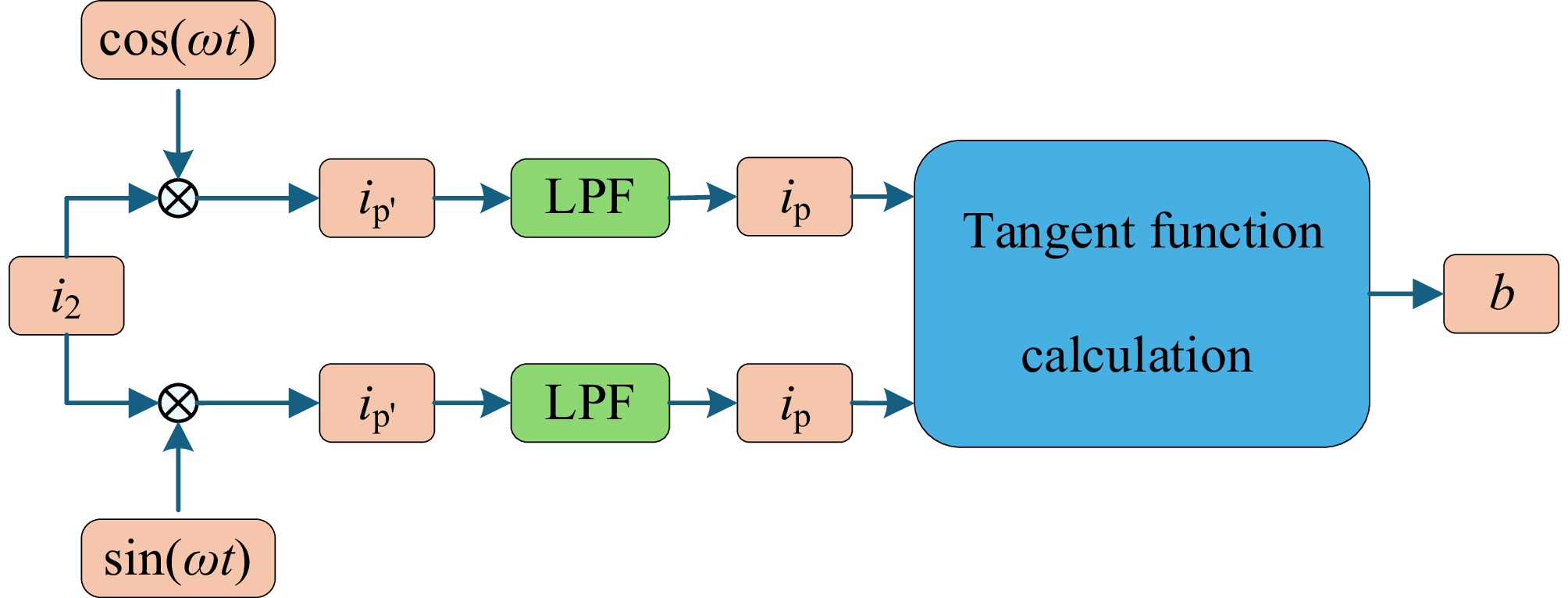
Figure 4.
Schematic diagram of active and reactive current decomposition for phase angle estimation.
-
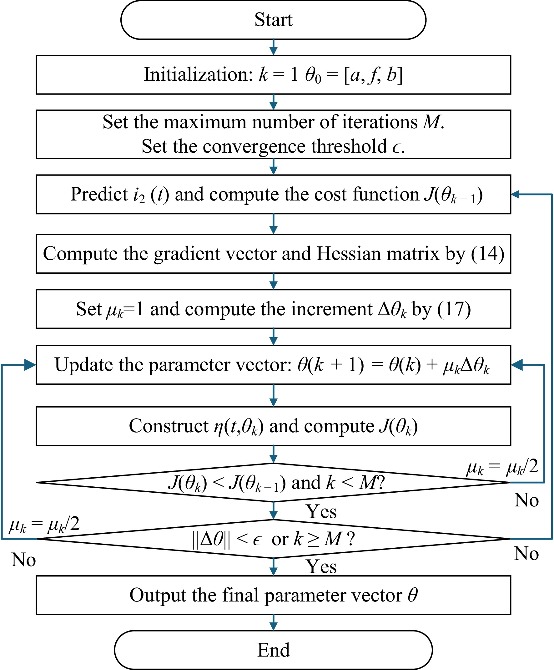
Figure 5.
Flowchart of parameter estimation for amplitude, frequency, and phase using the GN iterative algorithm.
-
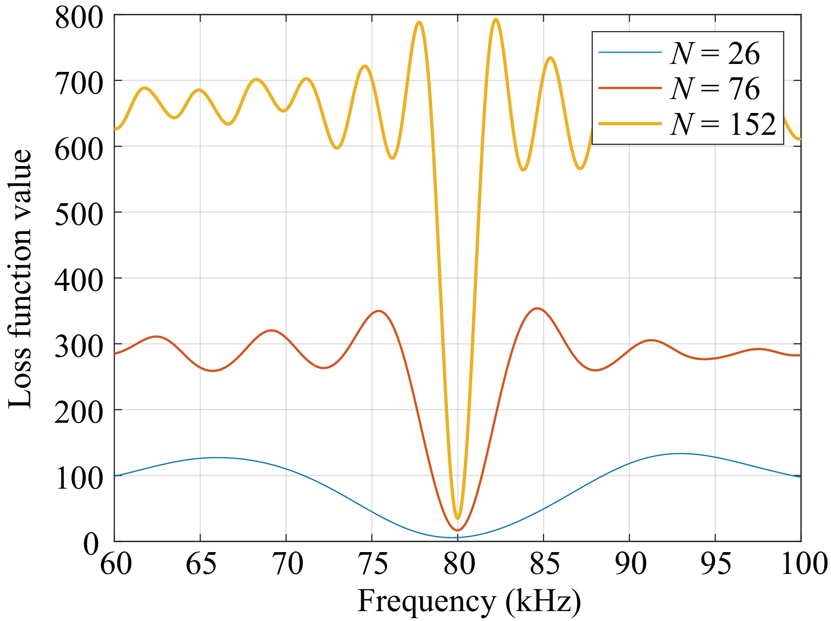
Figure 6.
Waveforms of the loss function under different data lengths.
-
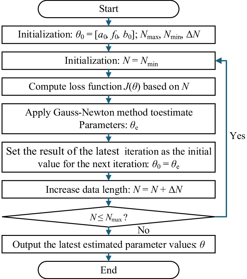
Figure 7.
Flowchart of iterative parameter estimation using the GN iterative algorithm with increasing data length.
-
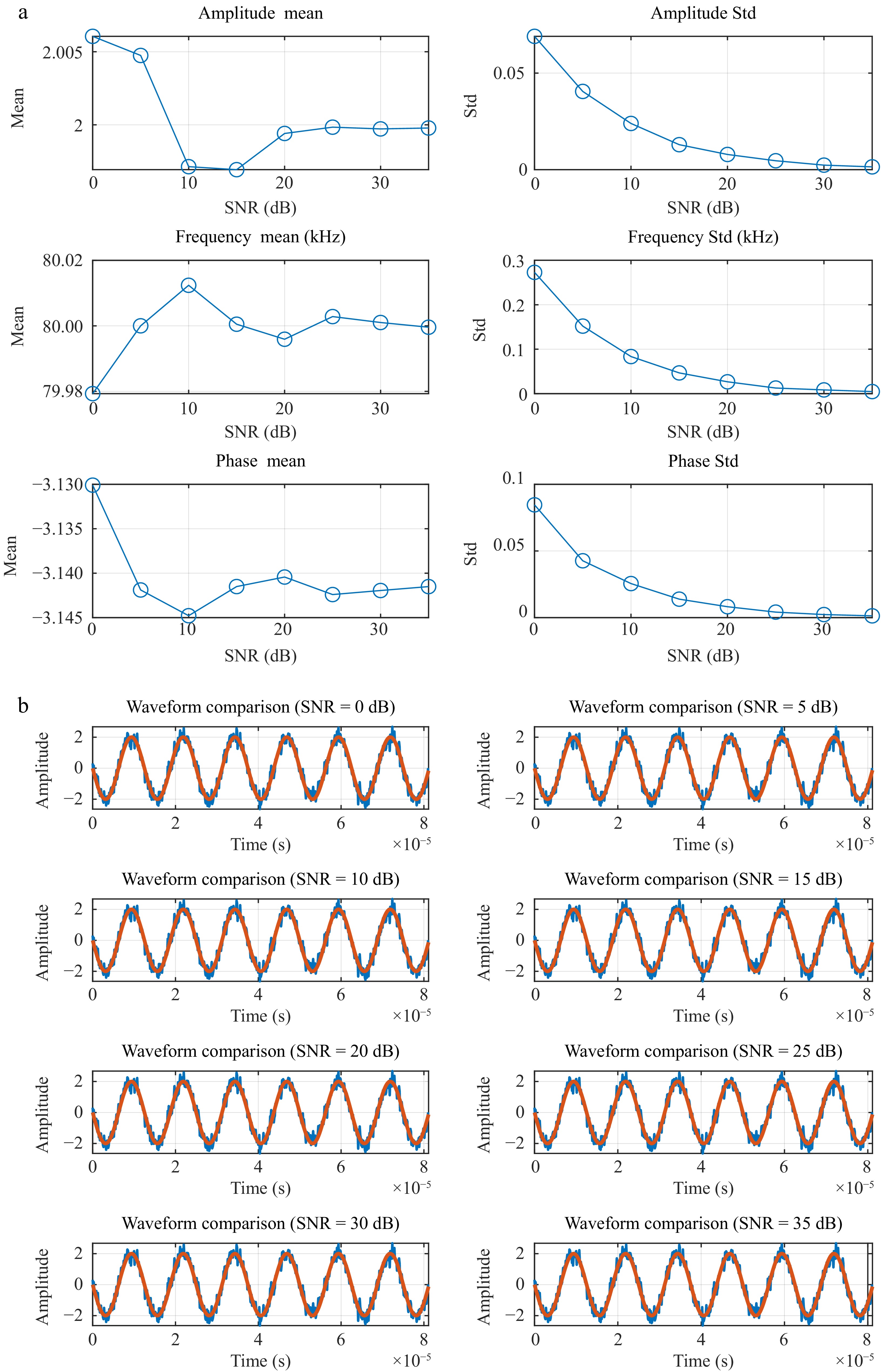
Figure 8.
Parameter estimates obtained under different SNRs. (a) Parameter estimates under different SNRs. (b) Comparion of the sampled noisy data and the estimated ones.
-
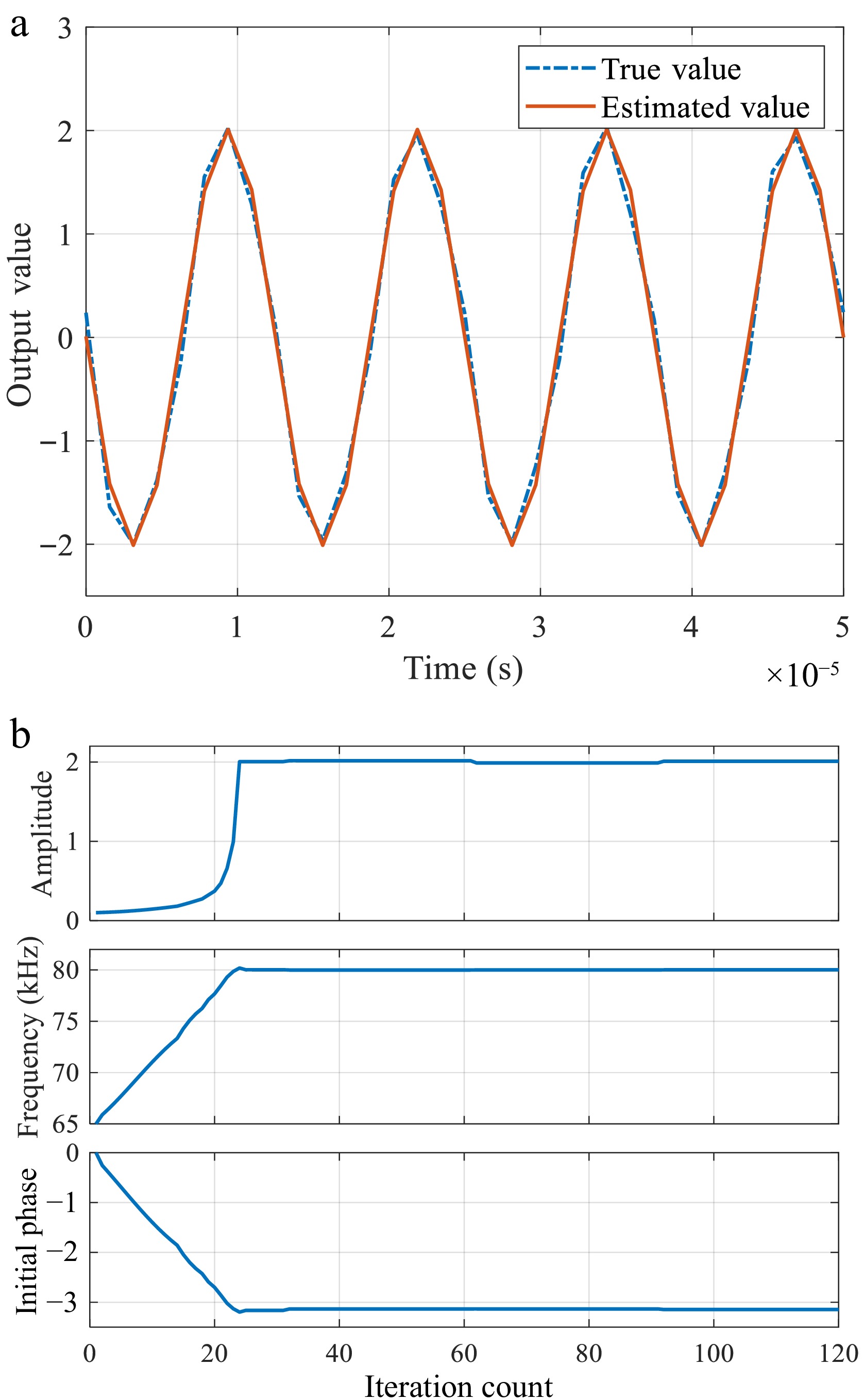
Figure 9.
Estimation results when the data length increases progressively. (a) Comparison of the sine waveform based on the final parameter estimates with the original waveform. (b) Variance and mean of estimated parameters.
-
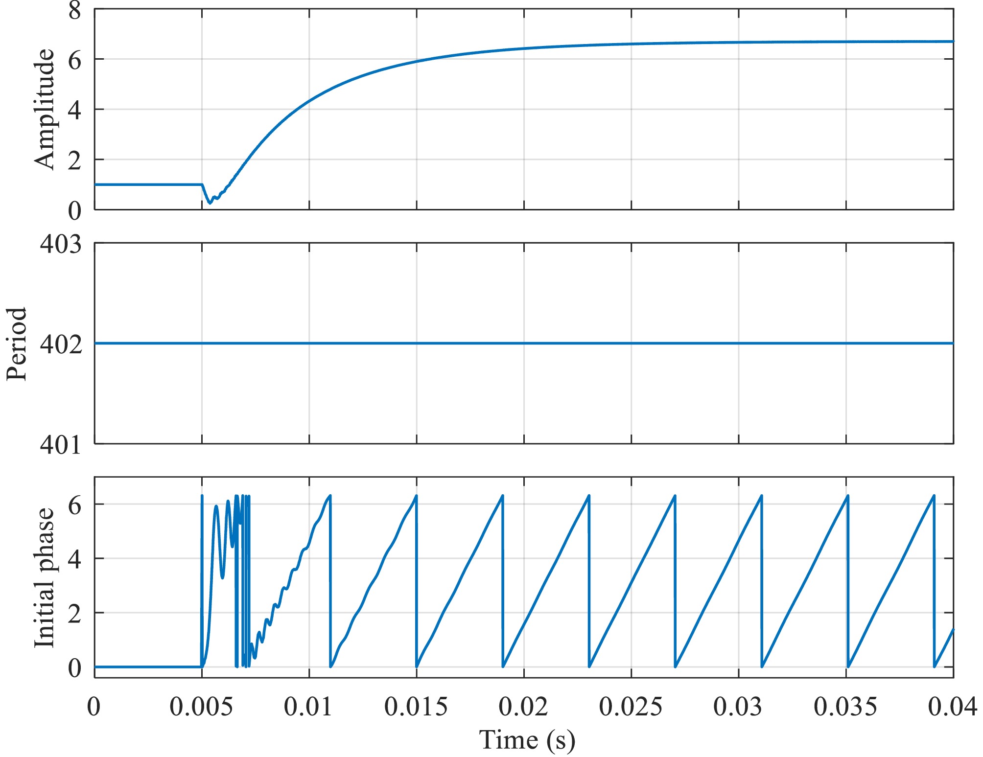
Figure 10.
Parameter estimates under primary-secondary frequency mismatch.
-
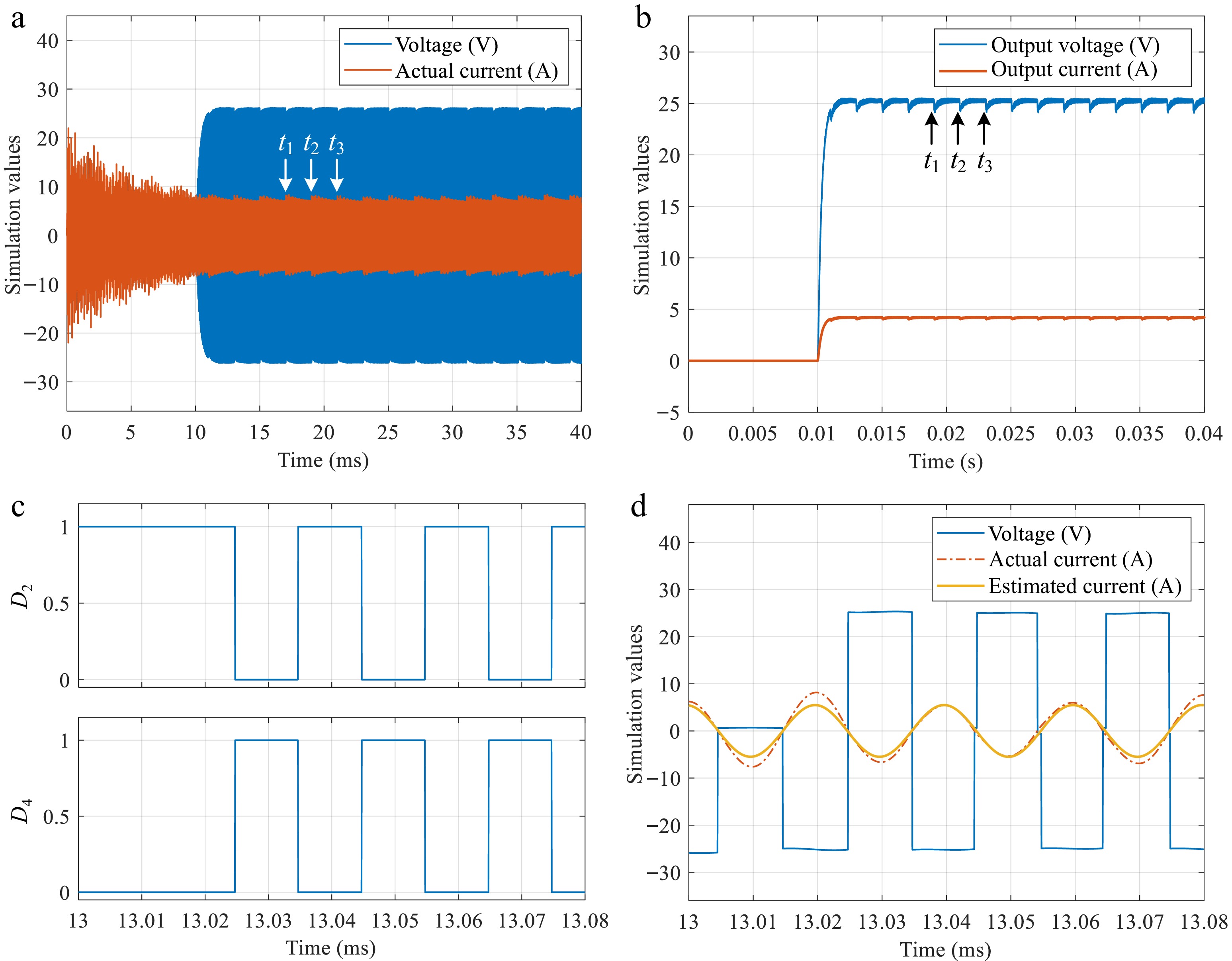
Figure 11.
Waveform under a primary-secondary frequency mismatch. (a) Waveform of voltage
${v_2}$ ${i_2}$ ${R_{\text{L}}}$ ${D_2}$ ${D_4}$ ${v_2}$ ${i_2}$ ${i_2}$ -
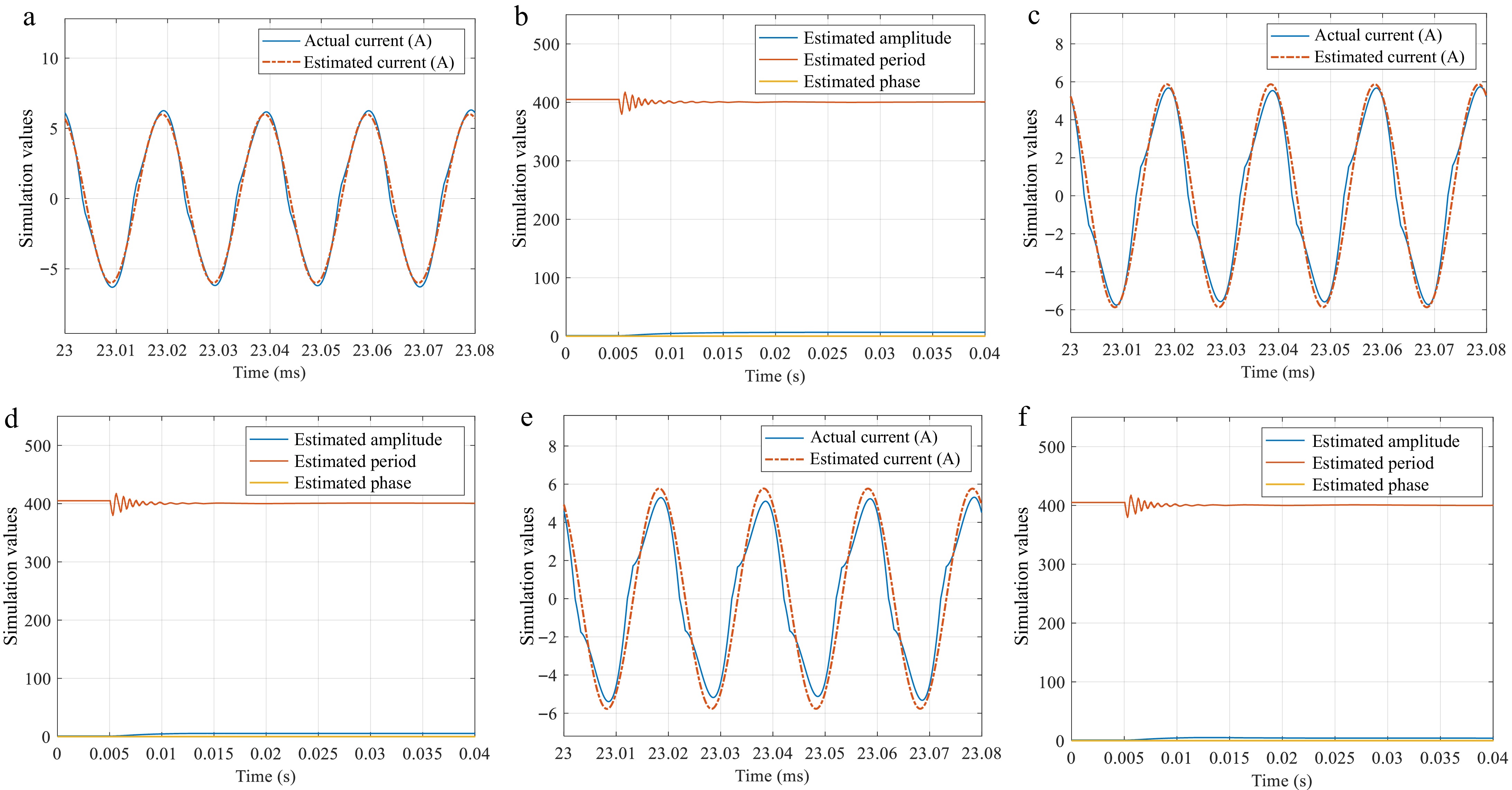
Figure 12.
Parameter estimates obtained under different levels of harmonic distortions. (a), (b):
${R_{\text{L}}} = 20\;\Omega $ ${R_{\text{L}}} = 40\;\Omega $ ${R_{\text{L}}} = 60\;\Omega $ -
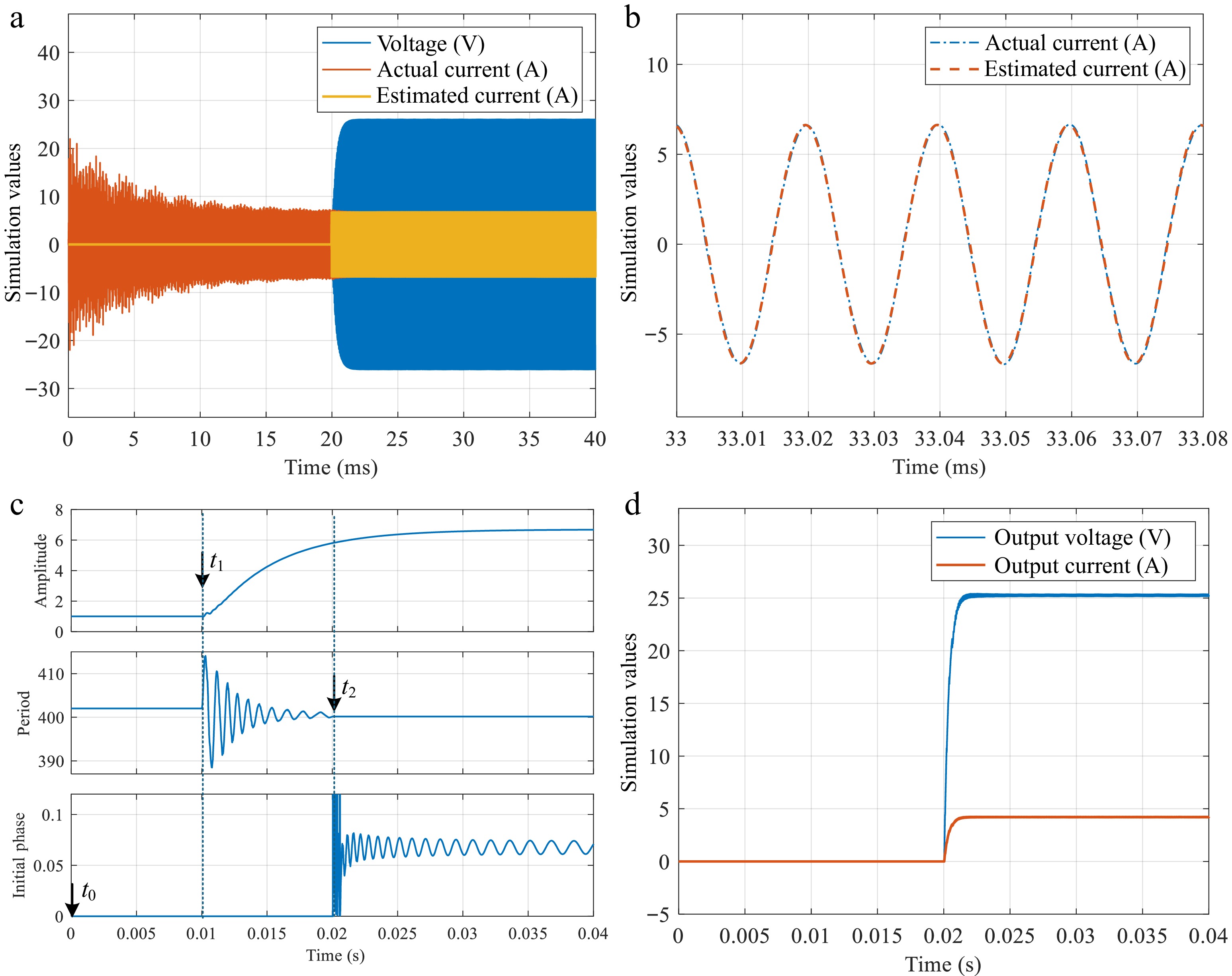
Figure 13.
Waveform of
${v_{\text{2}}}$ ${i_2}$ ${v_2},$ ${i_2}$ ${i_2}$ ${i_2}$ ${i_2}$ ${R_{\text{L}}}$ -
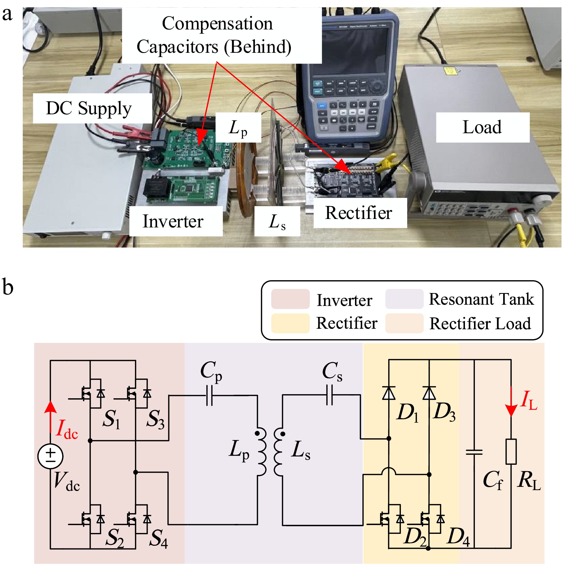
Figure 14.
SS compensated WPT system. (a) Prototype. (b) Circuit topology.
-
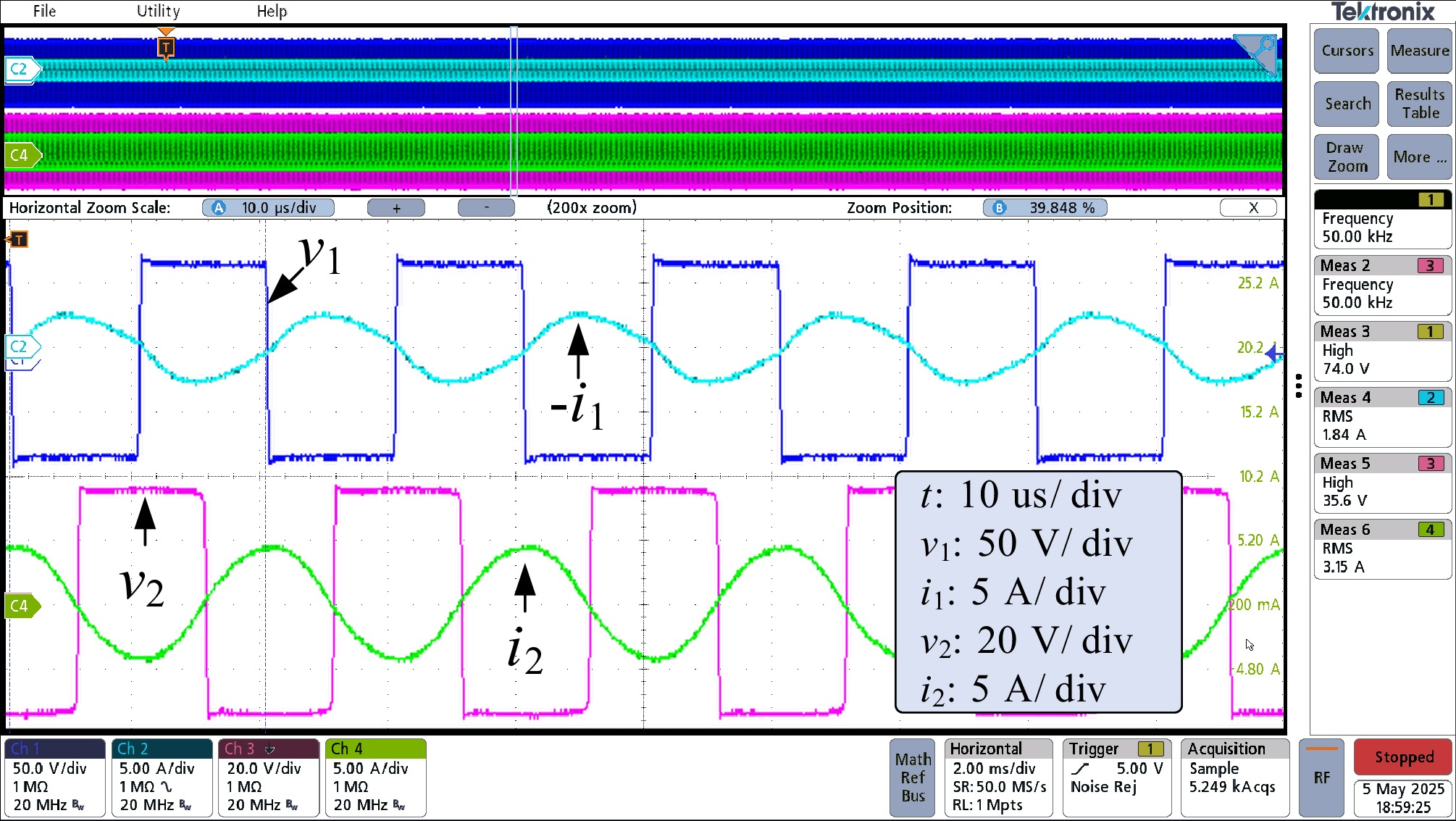
Figure 15.
Waveform of v1, i1, v2, and i2 in the diode bridge mode.
-
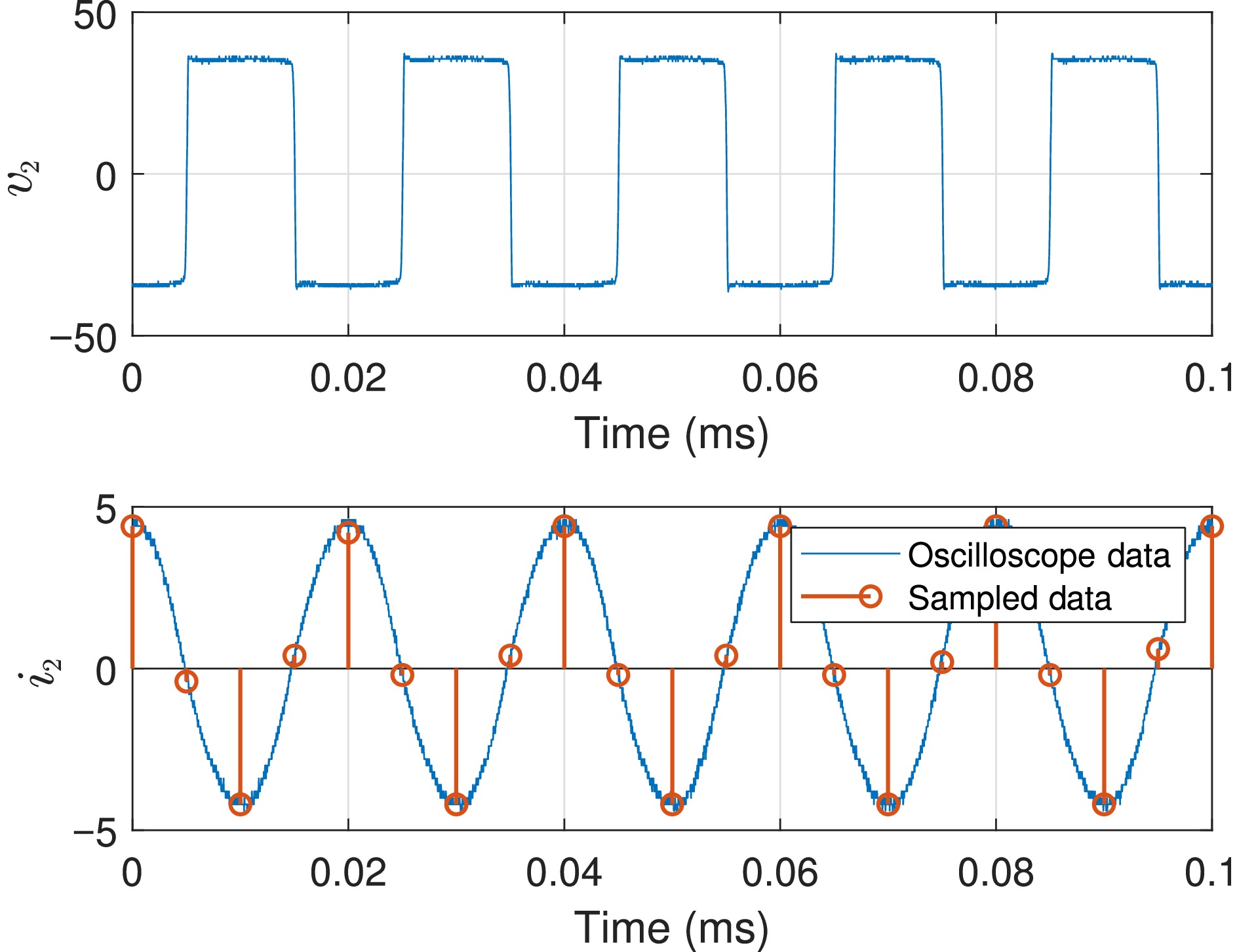
Figure 16.
Sampled data of i2 in the diode bridge mode.
-
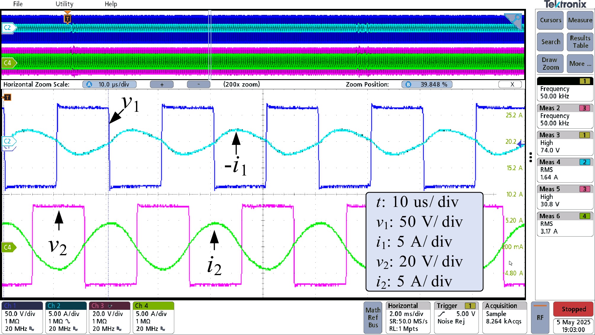
Figure 17.
Waveform of v1, i1, v2, and i2 in the active bridge mode, where the estimated secondary PWM frequency fs = 49.998 kHz is used.
-
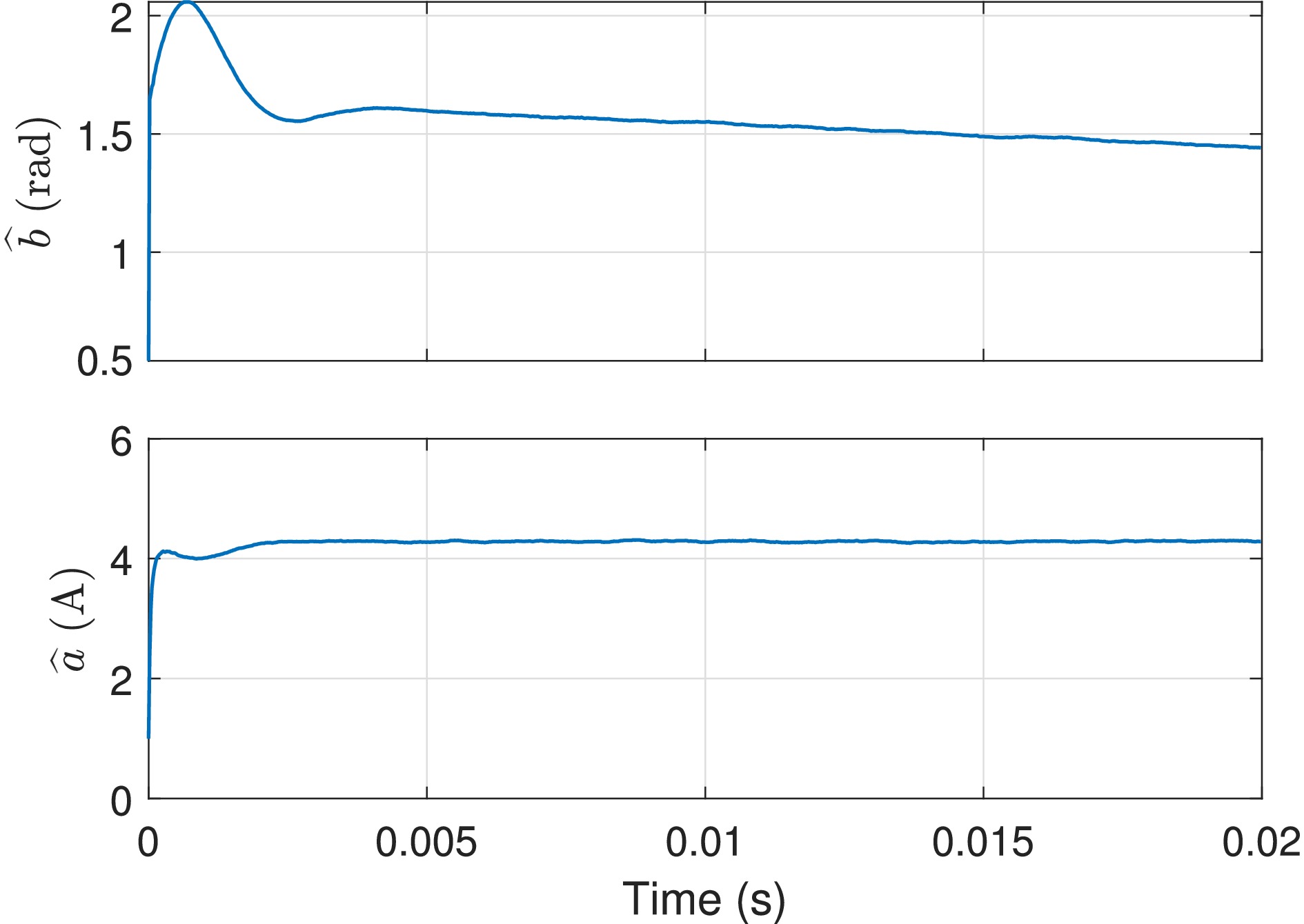
Figure 18.
Estimated parameters using the data presented in Fig. 17 (fs = 49.998 kHz).
-
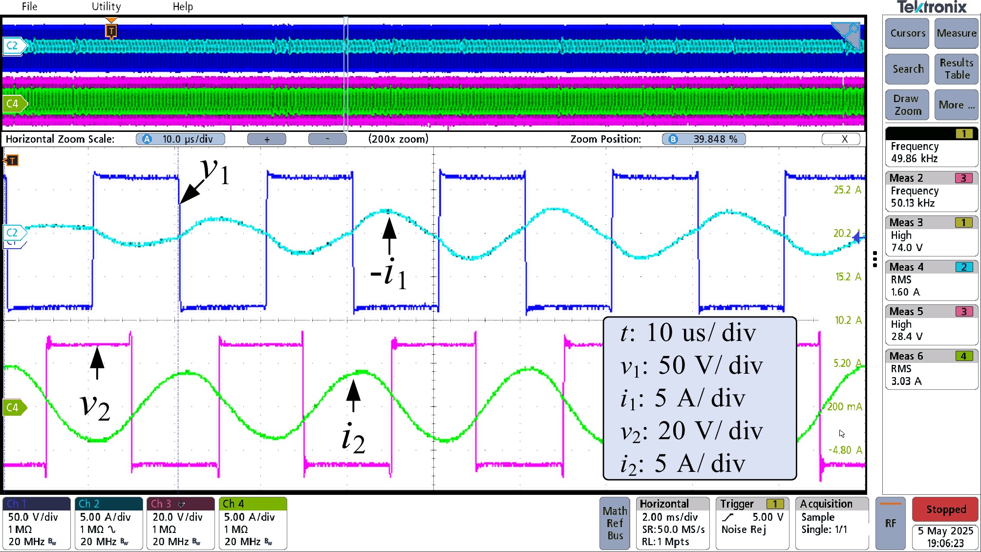
Figure 19.
Waveform of v1, i1, v2, and i2 in the active bridge mode with frequency mismatch (fs = 50.5 kHz).
-
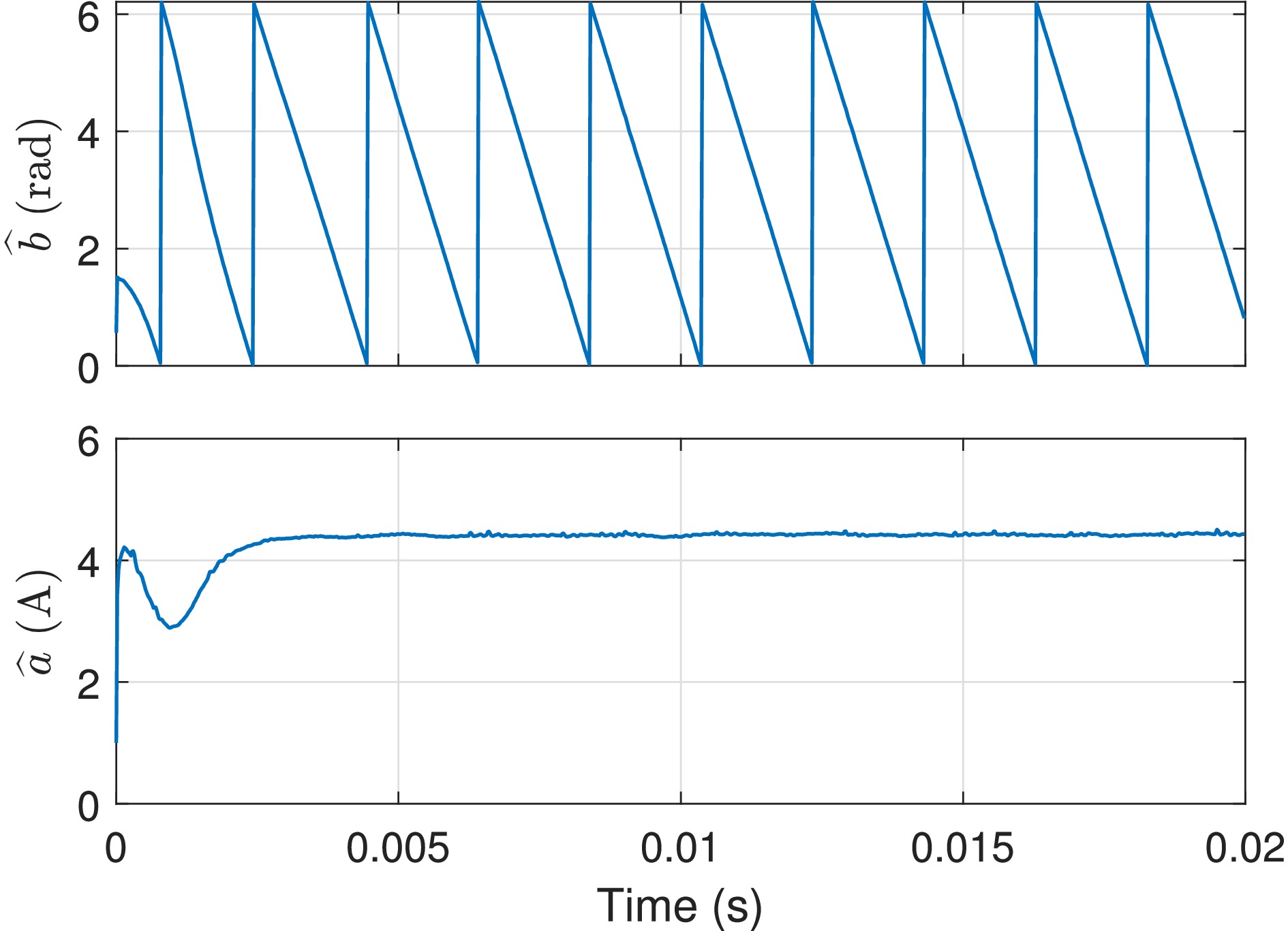
Figure 20.
Estimated parameters using the data presented in Fig. 19 (fs = 50.5 kHz).
-
N Var $(\hat a)$ Var $(\hat f)$ Var $(\hat b)$ 26 1.06 × 10⁻¹ 1.25 × 10⁸ 2.96 72 6.20 × 10⁻⁴ 3.73 × 10³ 5.95 × 10⁻⁴ 96 4.66 × 10⁻⁴ 1.57 × 10³ 4.52 × 10⁻⁴ 152 2.88 × 10⁻⁴ 3.86 × 10² 2.81 × 10⁻⁴ N Mean $(\hat a)$ Mean $(\hat f)$ Mean $(\hat b)$ 26 0.377565 77.886872 −2.727483 72 1.997164 80.044921 −3.157094 96 1.998176 80.008205 −3.141797 152 2.005136 80.003889 −3.143130 Table 1.
Variance and mean of estimated parameters for different data lengths.
-
SNR (dB) Parameter Ture value Mean Std 0 Amplitude 2 1.9937 8.13 × 10⁻² 5 Amplitude 2 1.9940 3.86 × 10⁻² 10 Amplitude 2 2.0012 2.62 × 10⁻² 15 Amplitude 2 2.0022 1.54 × 10⁻² 20 Amplitude 2 1.9994 7.29 × 10⁻³ 25 Amplitude 2 2.0006 4.73 × 10⁻³ 30 Amplitude 2 2.0001 2.36 × 10⁻³ 35 Amplitude 2 2.0002 1.29 × 10⁻³ 0 Frequency 80 80.022 267.36 5 Frequency 80 79.984 150.09 10 Frequency 80 80.014 82.733 15 Frequency 80 79.995 52.128 20 Frequency 80 79.999 26.779 25 Frequency 80 79.999 13.707 30 Frequency 80 80.000 8.5463 35 Frequency 80 80.000 4.4373 0 Phase −π −3.1518 7.95 × 10⁻² 5 Phase −π −3.137 4.16 × 10⁻² 10 Phase −π −3.1463 2.47 × 10⁻² 15 Phase −π −3.1412 1.55 × 10⁻² 20 Phase −π −3.1411 7.65 × 10⁻³ 25 Phase −π −3.1411 3.99 × 10⁻³ 30 Phase −π −3.1416 2.67 × 10⁻³ 35 Phase −π −3.1416 1.33 × 10⁻³ Table 2.
Estimated parameters.
-
Symbol Item Value Cp Primary side compensation capacitor 80 nF Cf1 Primary side parallel capacitor 120 nF Cs Secondary side compensation capacitor 80 nF Cf2 Secondary side parallel capacitor 120 nF Cf Output filter capacitor 50 nF Lp Primary side coil self-inductance 200 μH Ls Secondary side coil self-inductance 200 μH Lf1 Primary side compensation inductance 80 μH Lf2 Secondary side compensation inductance 80 μH M Mutual inductance 55 μH RL Load resistance 6 (default)/20/40/60 Ω Vdc DC power supply 200 V Table 3.
Main parameters of the LCC-LCC WPT system.
-
Symbol Item Value Cp Primary side compensation capacitor 50.1 nF Cs Secondary side parallel capacitor 50.2 nF Cf Output filter capacitor 504.4 μF Lp Primary coil self-inductance 209.2 μH Ls Secondary coil self-inductance 204.4 μH M Mutual inductance 66.5 μH RL Load resistance 10 Ω Vdc DC power supply 74 V Table 4.
Main parameters of the SS WPT system.
Figures
(20)
Tables
(4)