-
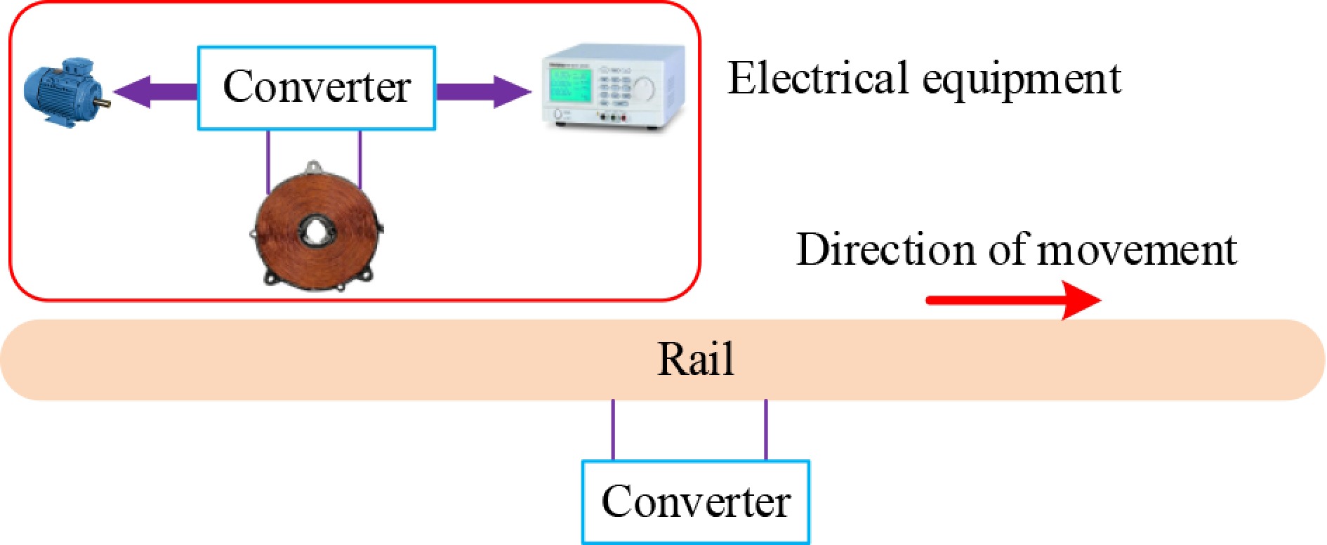
Figure 1.
Single rail power supply mode.
-
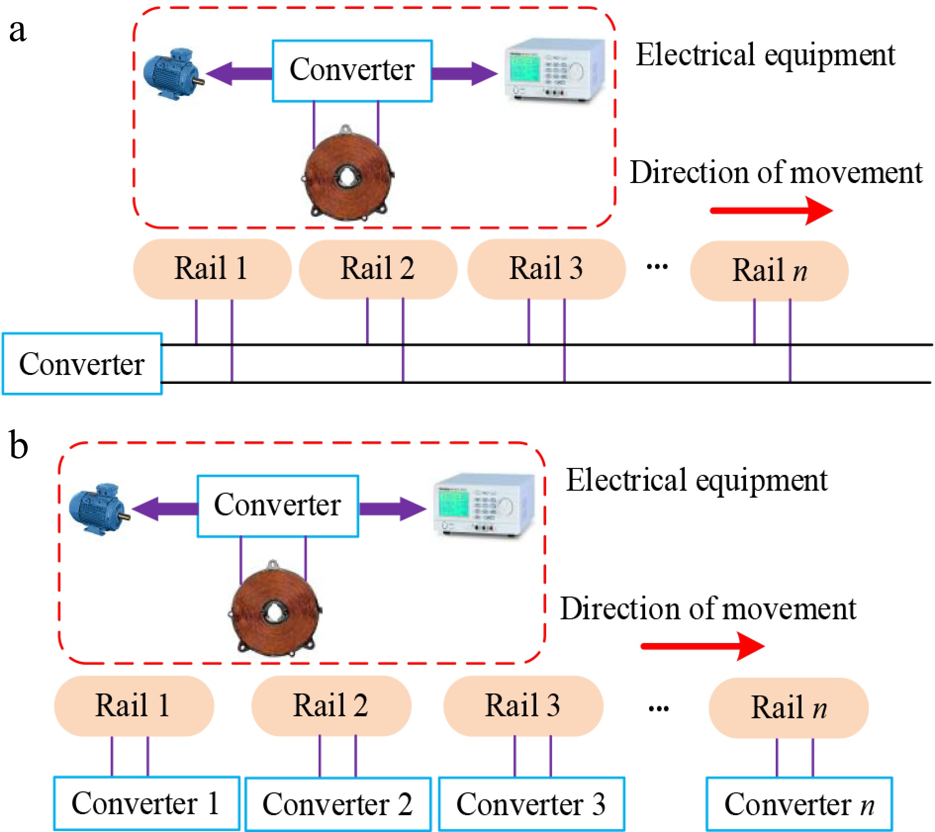
Figure 2.
Segmented rail (multi-coil array) supply mode. (a) Single converter power supply mode. (b) Multiple converter power supply mode.
-
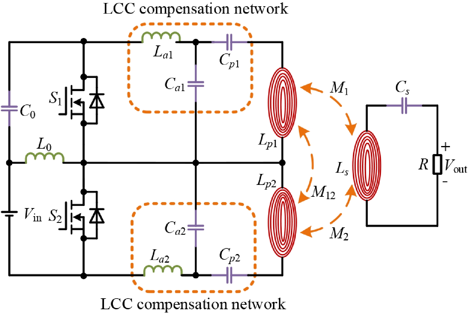
Figure 3.
Main circuit of the proposed dual-output inverter with wide soft-switching range for dynamic wireless charging of electric vehicles.
-
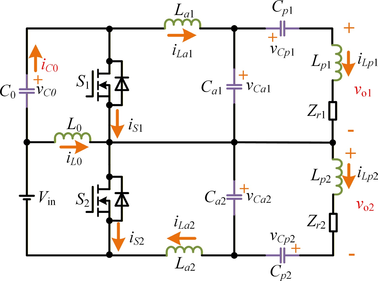
Figure 4.
Equivalent circuit of Fig. 3.
-
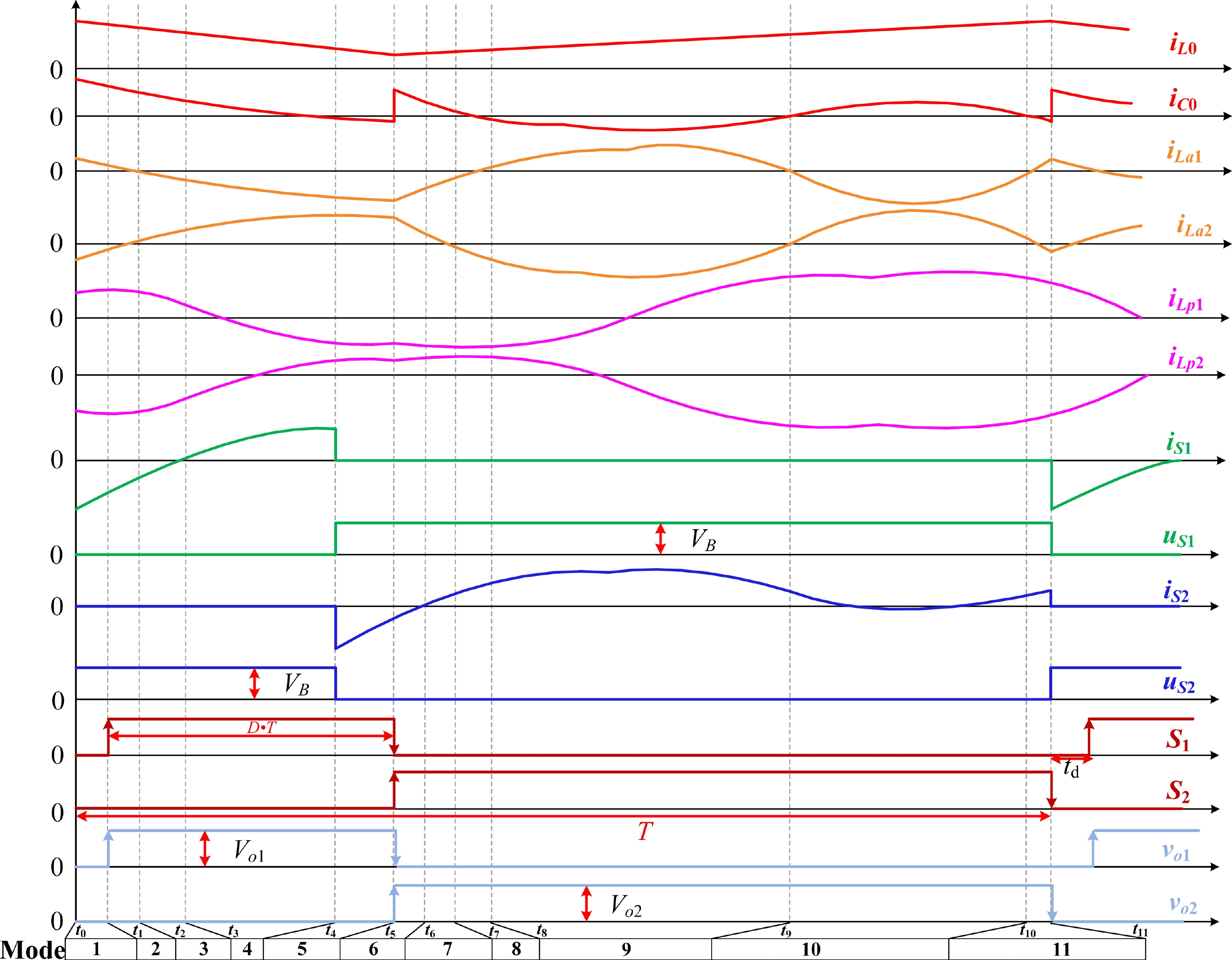
Figure 5.
Theoretical operating waveforms of key components.
-
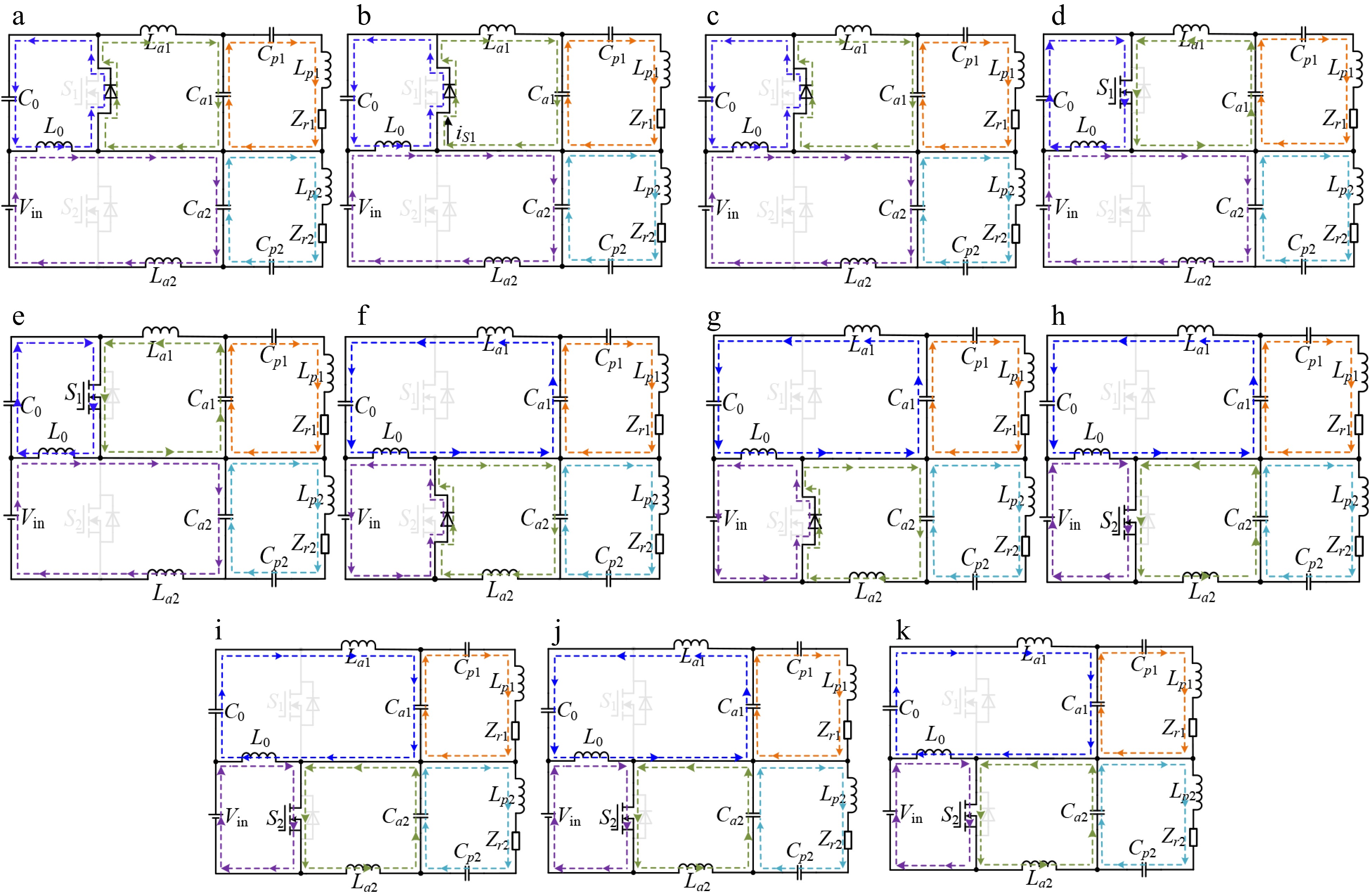
Figure 6.
Equivalent circuits in each of the operating modes. (a) Mode 1; (b) Mode 2; (c) Mode 3; (d) Mode 4; (e) Mode 5; (f) Mode 6; (g) Mode 7; (h) Mode 8; (i) Mode 9; (j) Mode 10; (k) Mode 11.
-
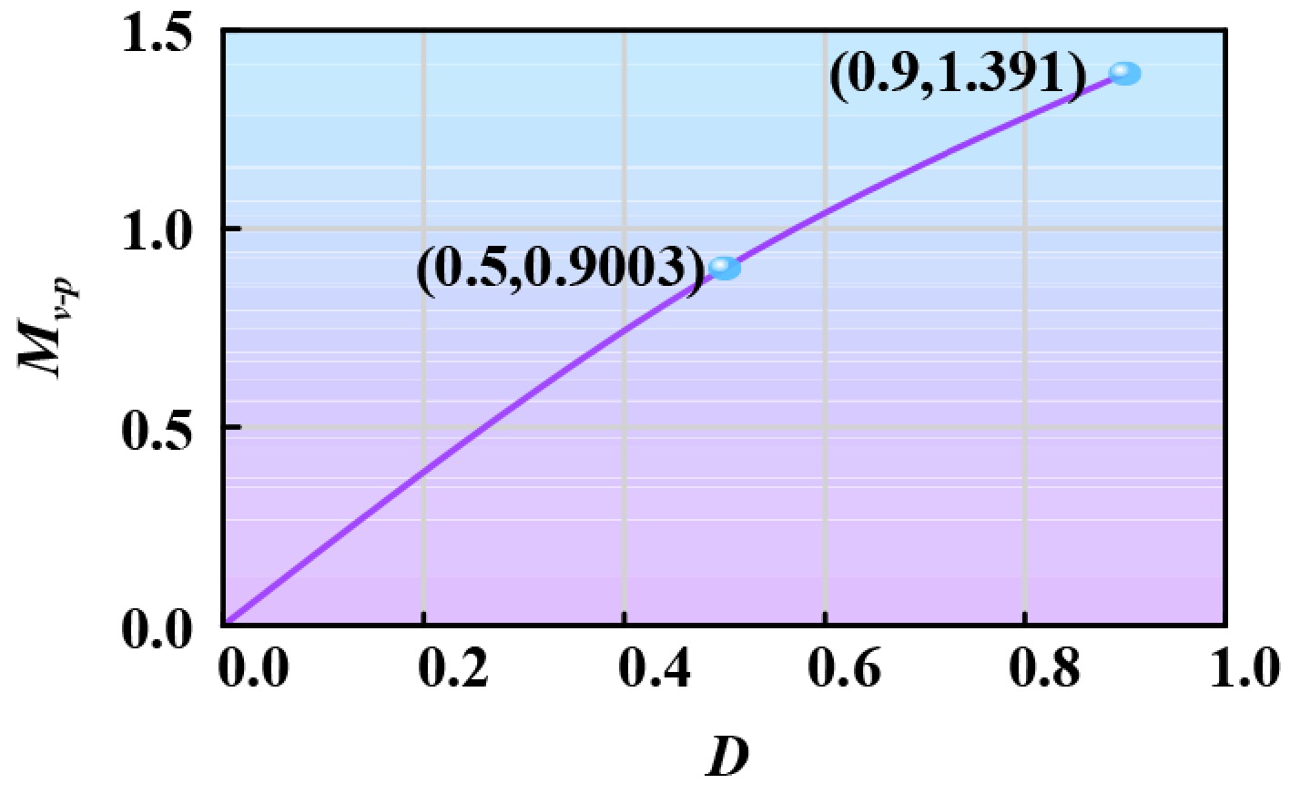
Figure 7.
The relationship between Mv-p and D.
-
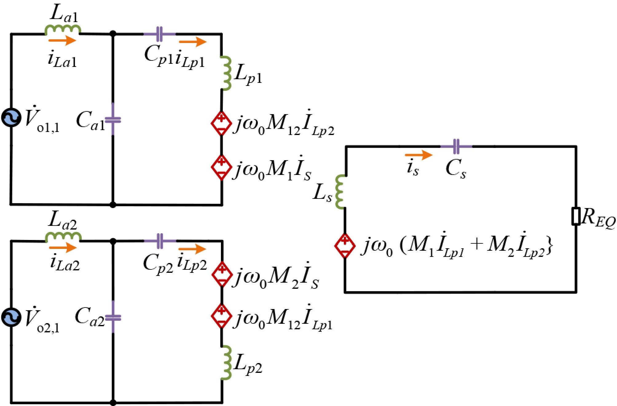
Figure 8.
The mutual inductance equivalent circuit in Fig. 3.
-
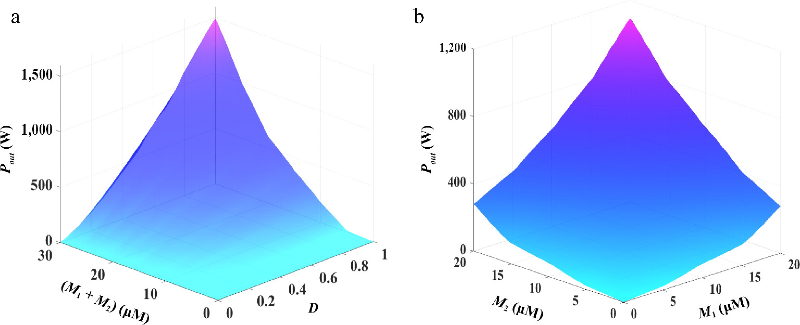
Figure 9.
The relationship among Pout with D, M1, and M2. (a) The relationship among Pout with D and M1 + M2. (b) The relationship among Pout with M1 and M2.
-
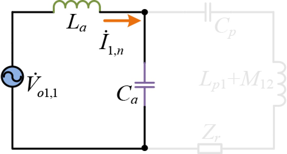
Figure 10.
Simplified model of LCC network under high order harmonics.
-
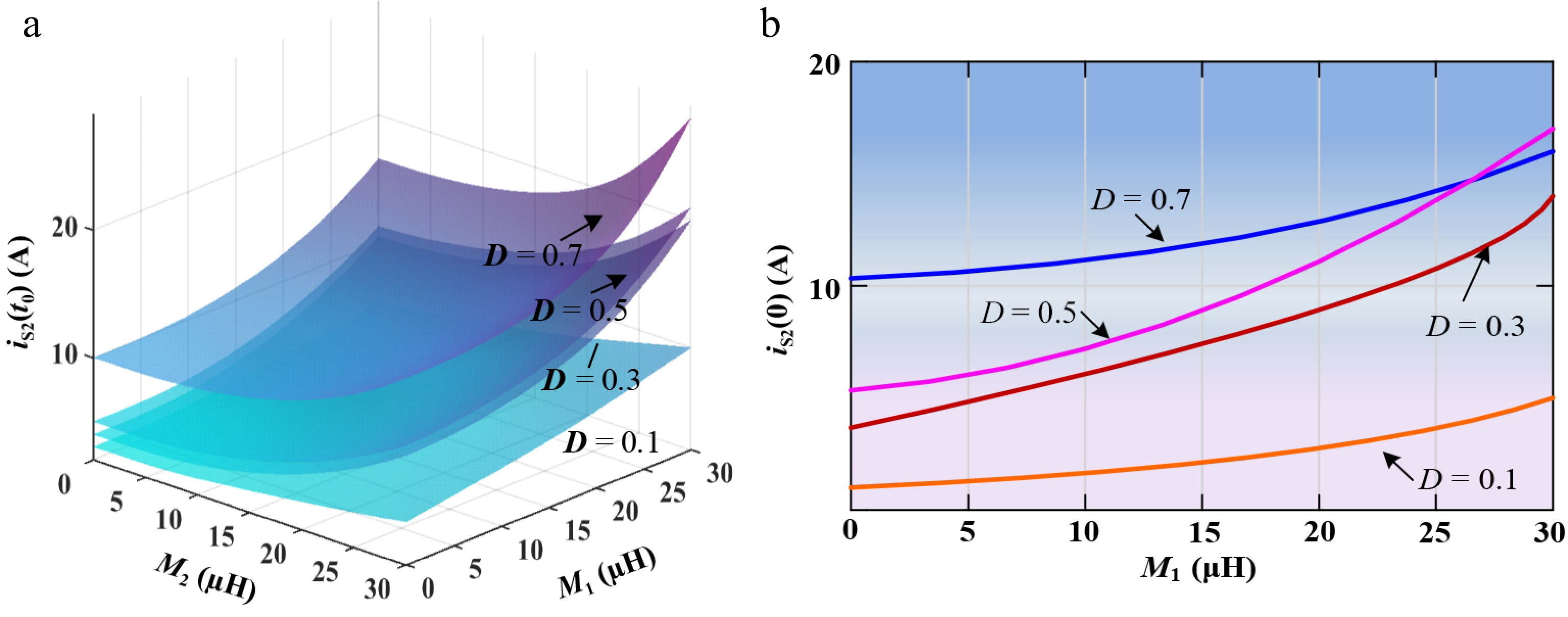
Figure 11.
The relationship among iS2(t0) with D, M1, and M2. (a) The relationship among iS2(t0) with D, M1, and M2 under different duty cycle conditions; (b) Cross-sectional view of (a) when M2 = 15 μH.
-
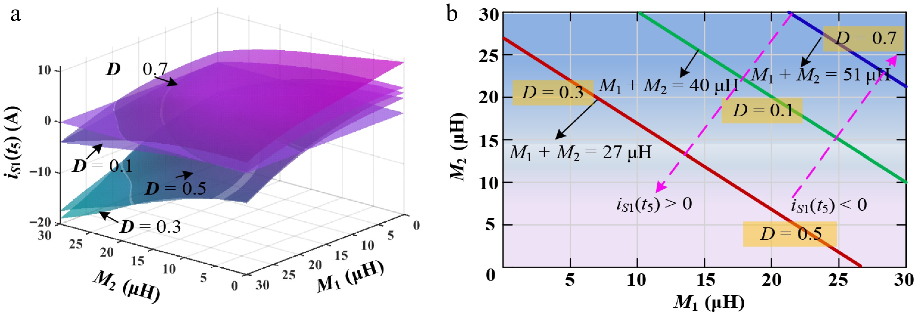
Figure 12.
The relationship among iS1(t5) with D, M1, and M2. (a) The relationship among iS1(t5) with D, M1, and M2 under different duty cycle conditions; (b) Polarity boundary line of iS1(t5).
-
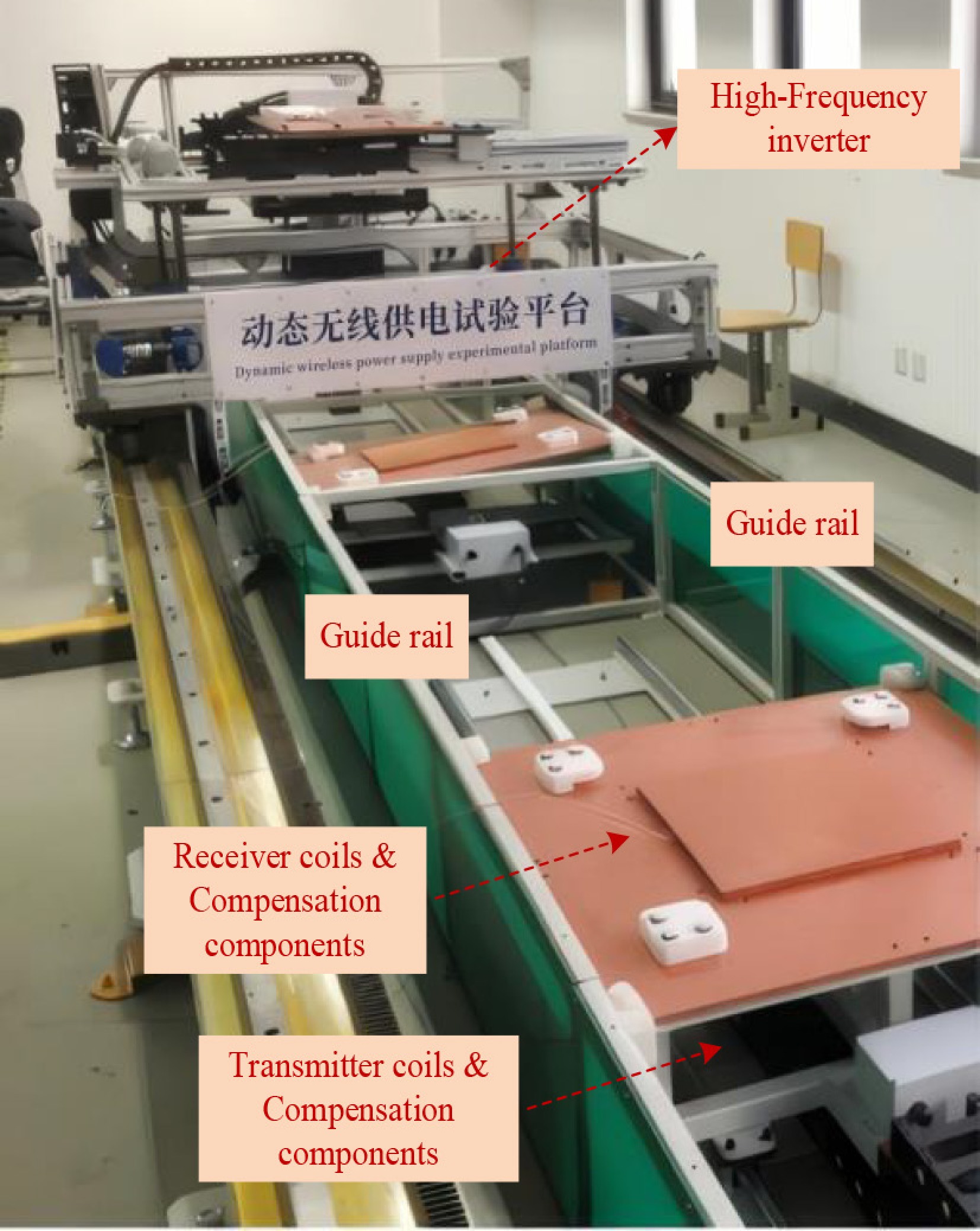
Figure 13.
Experimental platform.
-
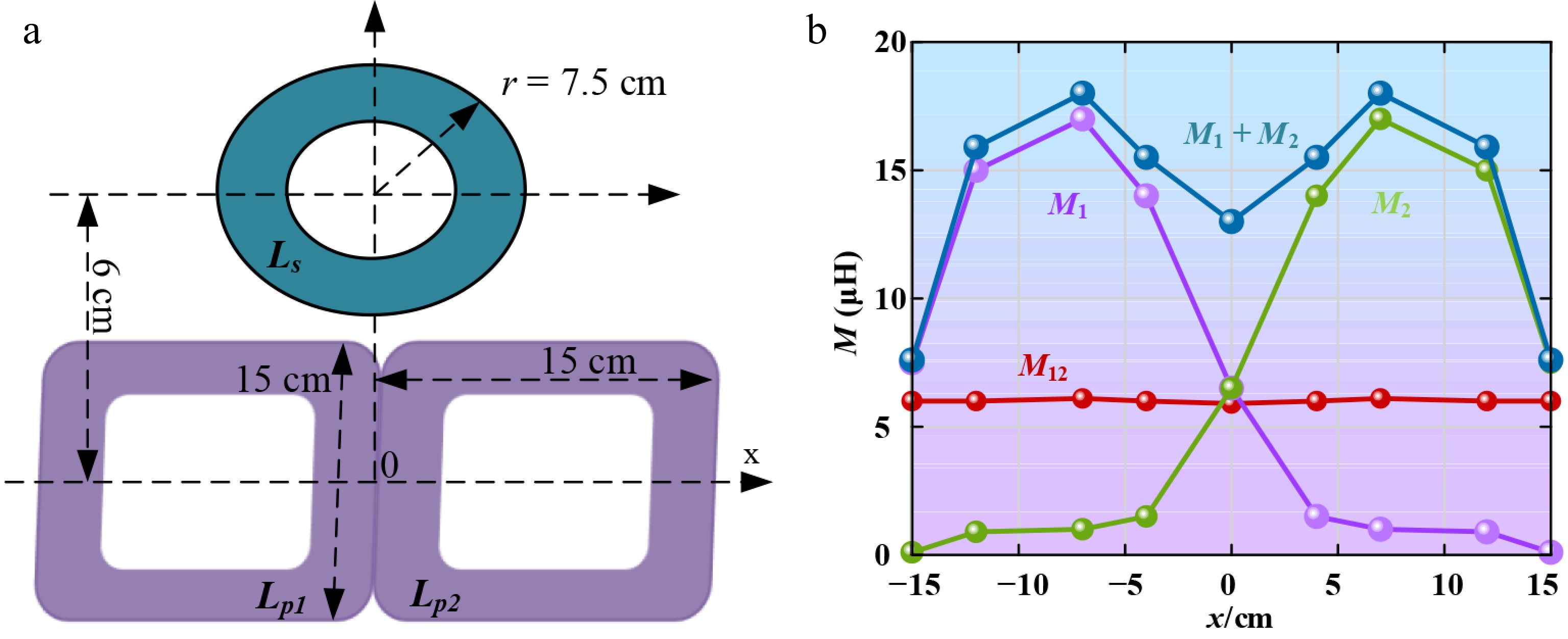
Figure 14.
The magnetic coupler. (a) Schematic diagram; (b) Measured mutual inductances vary with x-axis.
-
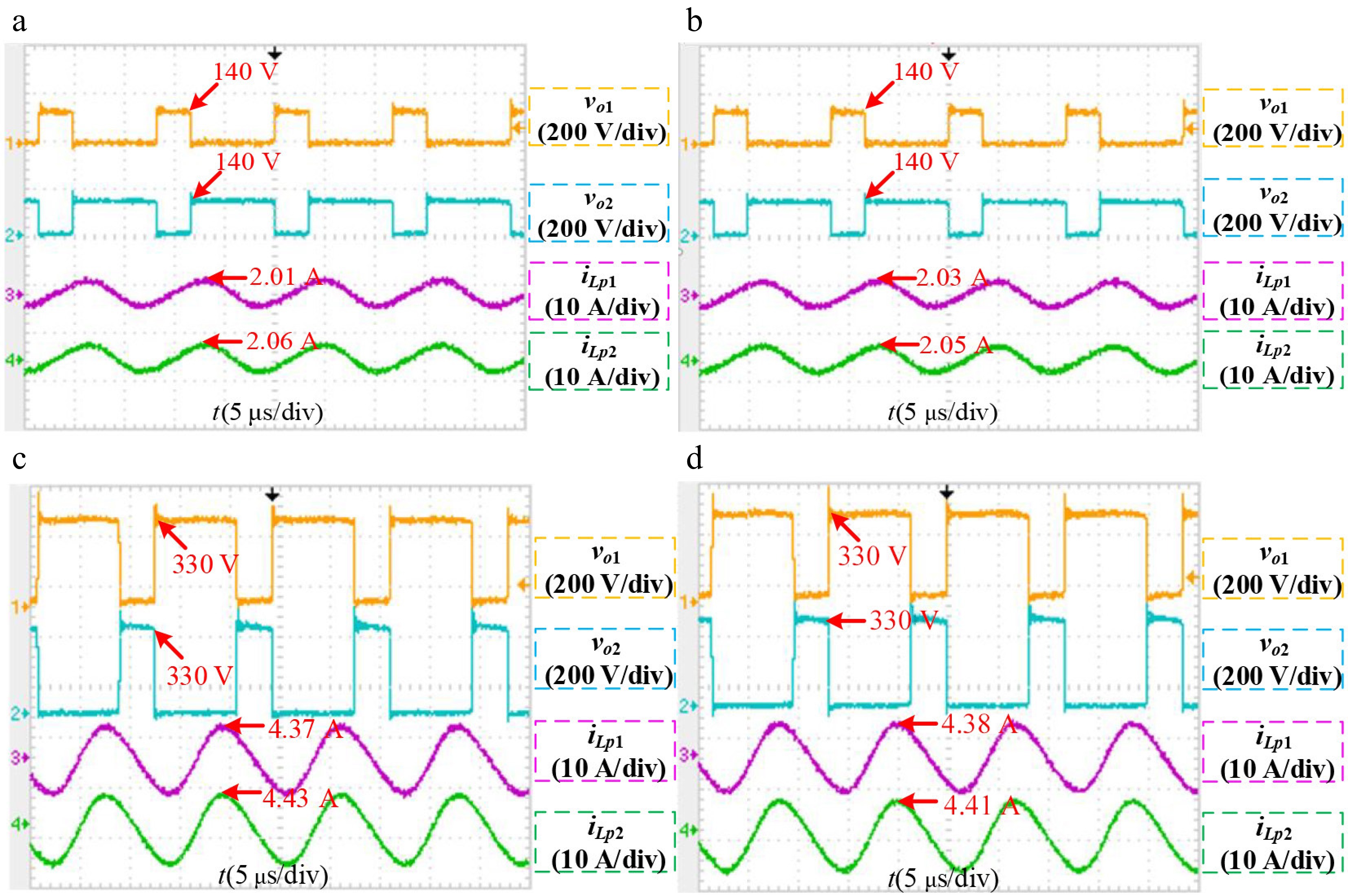
Figure 15.
Experimental waveforms of the inverter output voltages and primary coil currents. (a) x = 0, D = 0.3; (b) x = 7.5, D = 0.3; (c) x = 0, D = 0.7; (d) x = 7.5, D = 0.7.
-
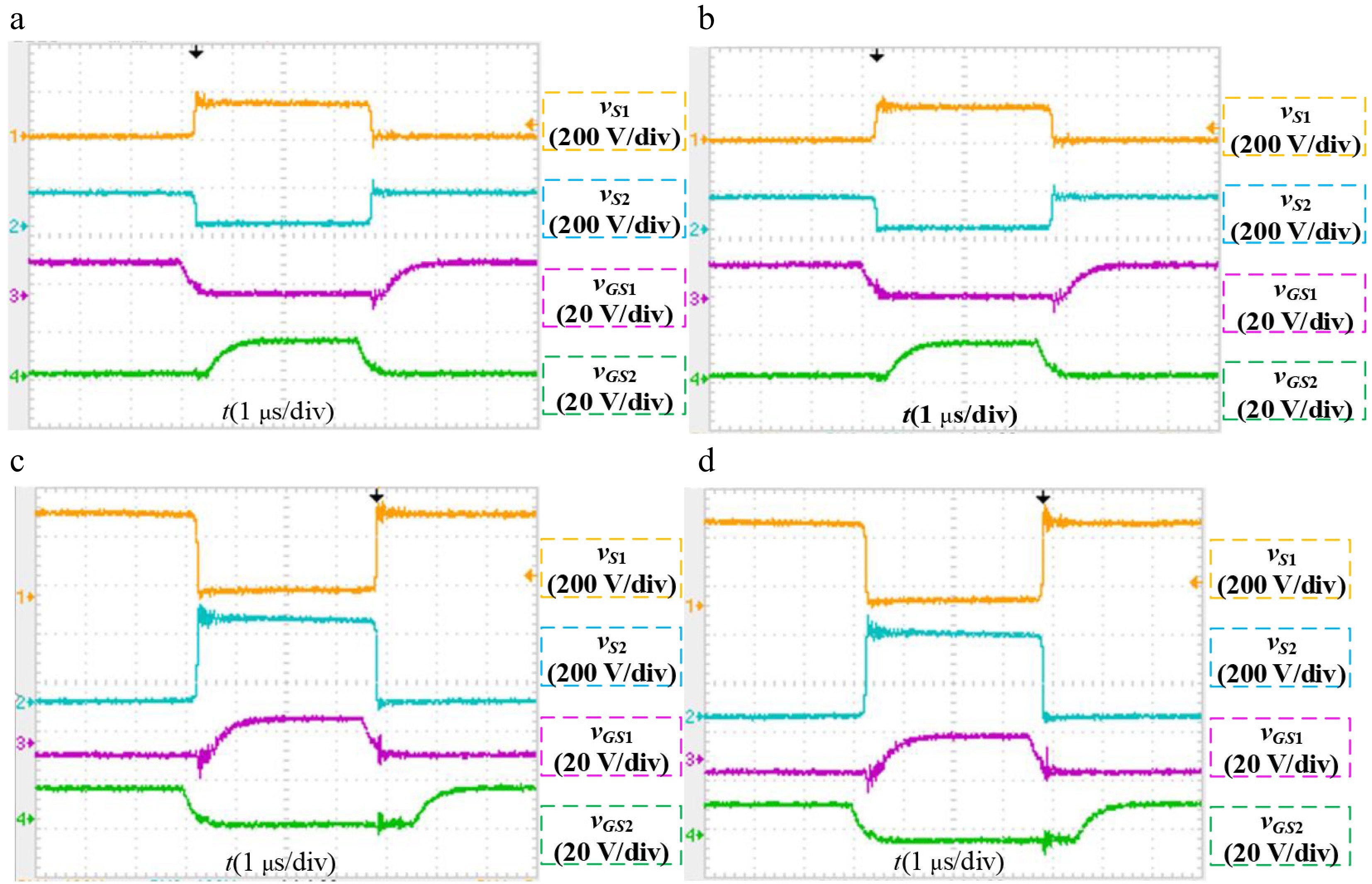
Figure 16.
Experimental waveforms of two switches. (a) x = 7.5, D = 0.3; (b) x = 0, D = 0.3; (c) x = 7.5, D = 0.7; (d) x = 0, D = 0.7.
-
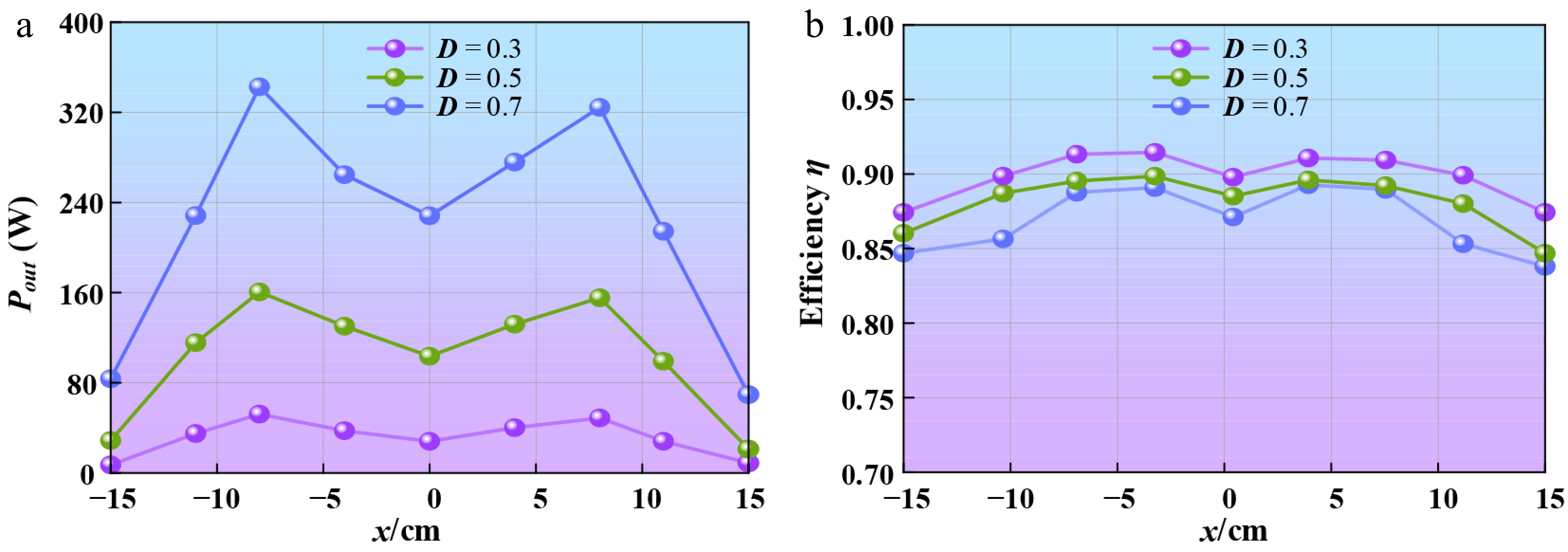
Figure 17.
Curves of the system output power and efficiency. (a) Output power; (b) Transfer efficiency.
-
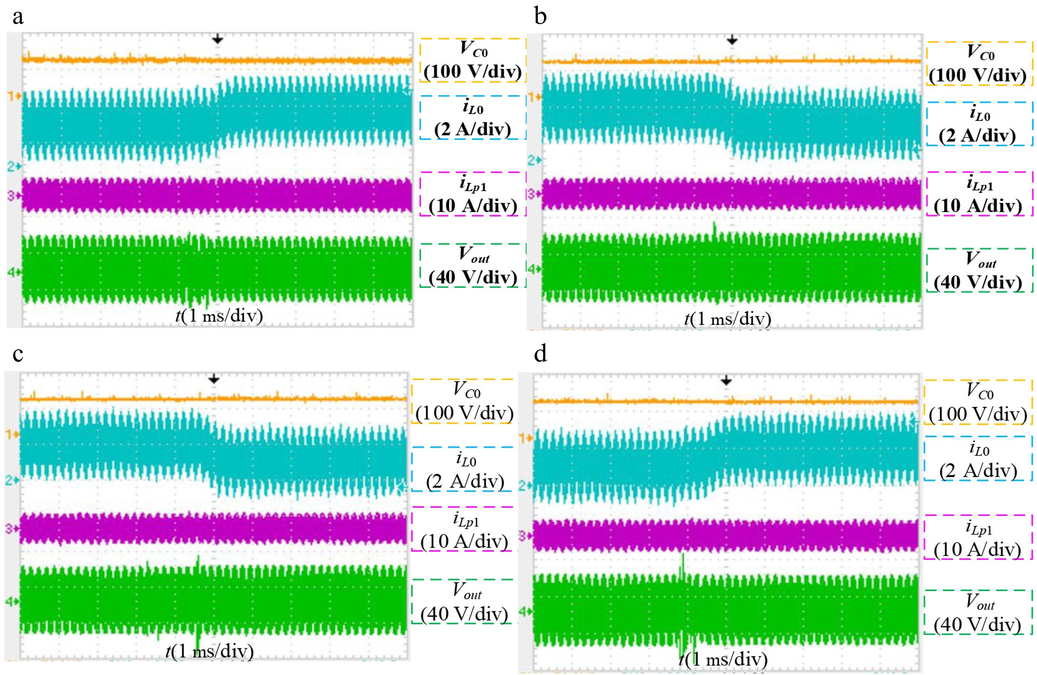
Figure 18.
Experimental waveforms of VC0, iL0, iLp1, and Vout under load change: (a) 5 to 3.3 Ω; (b) 3.3 to 5 Ω; (c) 5 to 10 Ω; (d) 10 to 5 Ω.
-
Type of inverter Voltage gain Number of input ports Number of output ports Number of switching devices Voltage type half bridge inverter 0~0.45 1 1 2 Voltage type full bridge inverter 0~0.9 1 1 4 Matrix converter 0~0.64 1 1 8 Multi-level inverter 0~1.35 1 1 8 Three-phase inverter 0~0.78 1 3 6 The proposed inverter 0~1.39 1 2 2 Table 1.
The comparison between the proposed dual output inverter and several typical inverters.
-
Parameter Value Parameter Value Vin 100 V La 50 μF Lp 100 μH Ca 70.12 nF L0 150 μH Cp 62.94 nF Ls 130 μH R 5 Ω C0 100 μF M12 5.7 μH Cs 26.97 nF f0 85 kHz Table 2.
Main system parameters.
Figures
(18)
Tables
(2)