


-
Wireless power transfer (WPT) is a technology that uses power electronics technology and modern control theory to achieve non-contact wireless transmission through soft media[1−3]. The World Economic Forum (WEF) has listed WPT as one of the top ten emerging technologies that have the greatest impact on the world and are most likely to provide answers to global challenges, for two consecutive years. It eliminates many problems associated with conventional contact power transmission methods, and solves the power supply problems of equipment in extreme, harsh, and complex environments (such as deep sea, deep space, flammable and explosive working environments). It meets people's requirements for safety, flexibility, and reliability of electrical equipment[4−7].
WPT technology is a research hotspot[8−10] due to its advantages of safety, convenience, flexibility, and freedom from structural and topological limitations[11,12]. In recent years, WPT technology has been gradually applied to mobile loads (such as wireless charging of electric vehicles, transport vehicles in logistics systems, transmission mechanisms in storage systems, and inspection robots in substations[13−15]), namely dynamic WPT systems. There are two common power supply modes shown in Figs. 1 and 2. Figure 1 illustrates the integrated single rail power supply mode[16,17]. When the electric equipment is driving above the transmitting rail, the receiver coil can obtain continuous energy. However, the disadvantage of the single-rail power supply mode is that the length of the energy transmitting rail is much larger than the size of the receiver coil, resulting in a small coupling coefficient and significant magnetic field exposure problems, making it unsuitable for long-distance applications. Figure 2 illustrates the power supply mode of the segmented rail (for ease of description, transmitting rails and transmitting coils are collectively referred to as transmitting rails subsequently). Multiple transmitting rails are laid in sequence on the moving path of the electric equipment, enabling segmented power supply of the mobile equipment and thus addressing the issues associated with the integrated single-rail power supply mode. In this power supply mode, there are two converter drive modes. In the single-converter drive mode shown in Fig. 2a[18], multiple transmitting rails share one converter, which can realize synchronous driving of multiple transmitting rails but requires an additional rail switching circuit to minimize losses from non-working rails. Simultaneously, this drive mode demands high converter capacity and has low system redundancy, making it not the optimal driving solution for long-distance applications. The multi-converter drive mode shown in Fig. 2b can achieve the independent control of each transmitting rail, with higher system redundancy, making it more suitable for long-distance applications[19]. However, this drive mode requires a large number of converters, increasing system cost, and maintenance complexity.
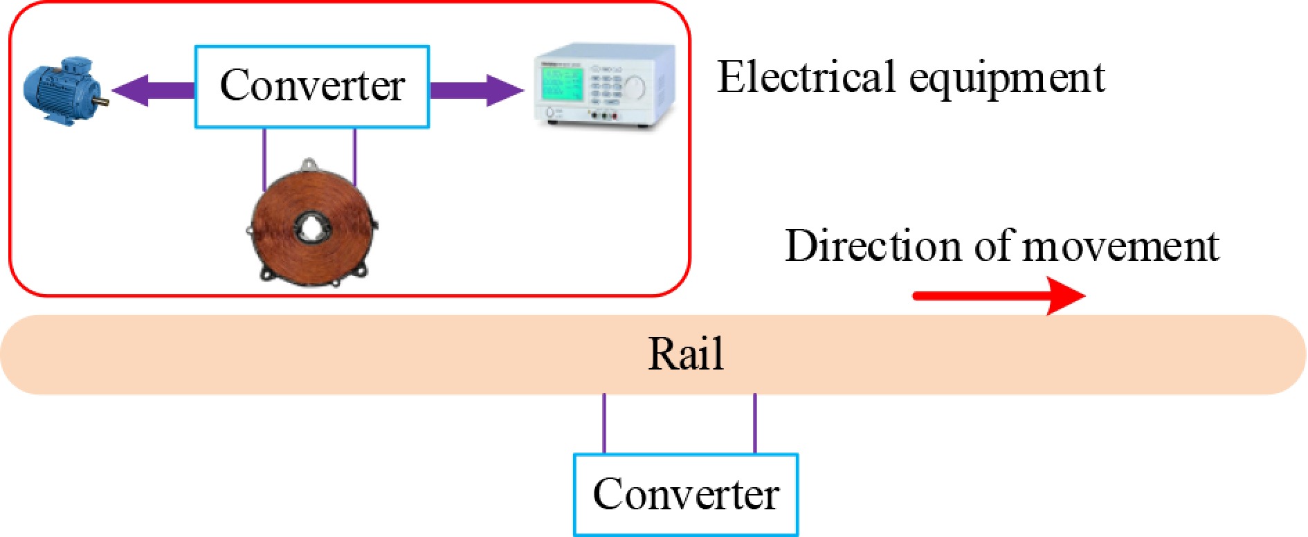
Figure 1.
Single rail power supply mode.
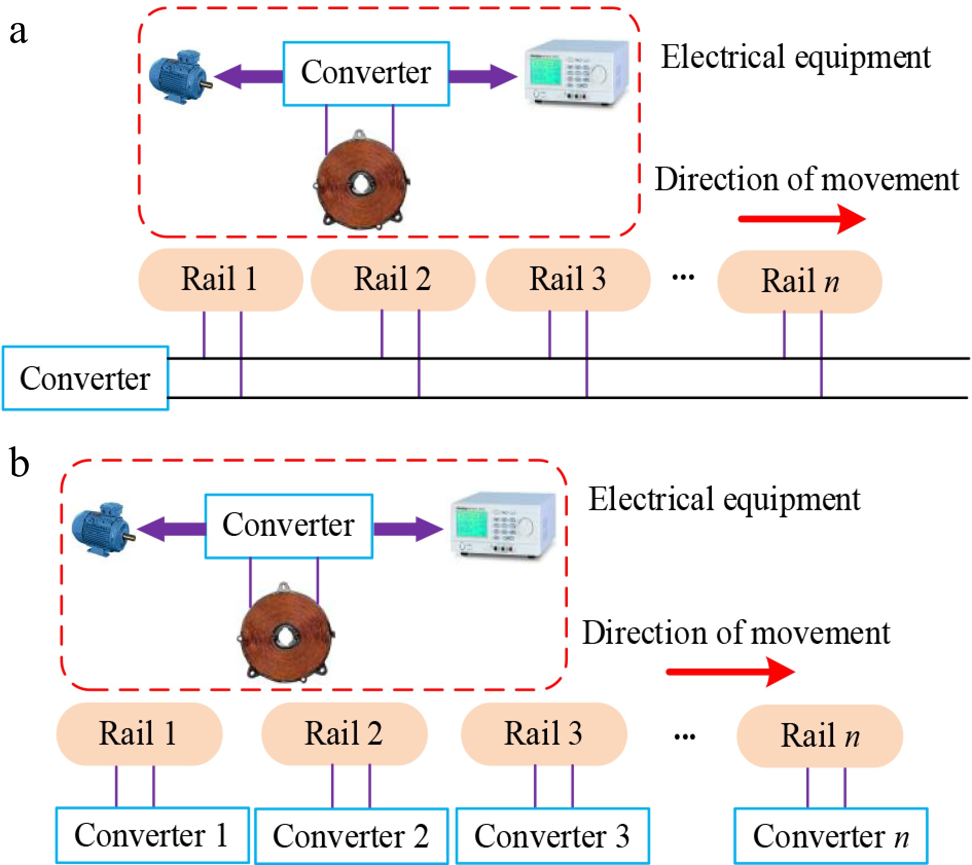
Figure 2.
Segmented rail (multi-coil array) supply mode. (a) Single converter power supply mode. (b) Multiple converter power supply mode.
As a power converter for WPT systems, in addition to the commonly used bridge, push-pull and class-E inverters, reported topologies include matrix converters[20], multi-level inverters[21], three-phase inverters[22−24], and parallel multiple inverters[25], etc. Research on these topologies mainly focuses on enhancing system power. They all involve a larger number of switching devices or DC energy storage components, and most are single-output topologies, which are more suitable for driving a single transmitting rail. As an integrated single-stage boost inverter, the high step-up inverter can realize boost and conversion between direct current and alternating current at the same time. It has the characteristics of a few switching devices, which is a simple structure and control strategy. It is often used to isolate DC-DC power supplies, photovoltaic inverters, and induction heating[26,27].
This paper proposes a high-frequency inverter with dual-output and wide-range soft-switching characteristics for dynamic wireless charging of electric vehicles. Compared with the multi-converter driving mode in Fig. 2b, the inverter can generate two identical outputs to drive two segments of transmitting rails, reducing the number of inverters and simplifying system control. On the other hand, compared with inverters commonly used in WPT systems, the proposed inverter can ensure the same voltage output capacity with fewer switching devices, further reducing the number of switching devices in a single inverter. It should be noted that the WPT system based on the proposed inverter is actually composed of multiple subsystems with the same structure and parameters, where each subsystem includes the proposed inverter and two segments of transmitting rails. The operation characteristics and rules of each subsystem are identical. This paper studies and analyzes a single subsystem, and the results are applicable to other subsystems, which can then be extended to the entire system.
-
The topology of the proposed dual-output ZVS inverter for WPT systems is illustrated in Fig. 3. Figure 4 is the equivalent circuit diagram of Fig. 3. In Fig. 4, the direction of each current indicated by the orange arrow is the positive reference direction, and the terminal of each voltage symbol '+' is the positive reference terminal. The dual-output inverter consists of two switches S1, S2, inductor L0, and capacitor C0. LCC resonant compensation network with constant current output characteristics is adopted at the energy transmitter, composed of compensation capacitors Ca1, Ca2, Cp1, Cp2, and compensation inductors La1 and La2. Ls denotes the receiver coil, Cs denotes the series resonant compensation capacitor, and R is the equivalent load resistance of the system. M12 denotes the cross mutual inductance between Lp1 and Lp2; M1 and M2 are the mutual inductance between Ls and Lp1, Lp2 respectively. Vin and Iin denote the input voltage and current of the inverter respectively. iS1 and iS2 denote the currents flowing through S1 and S2 respectively. iC0 and iL0 denote the current of C0 and L0 respectively, and vC0 denotes the voltage across C0. Zr1 and Zr2 are the equivalent reflection impedances of the two transmitter coils.
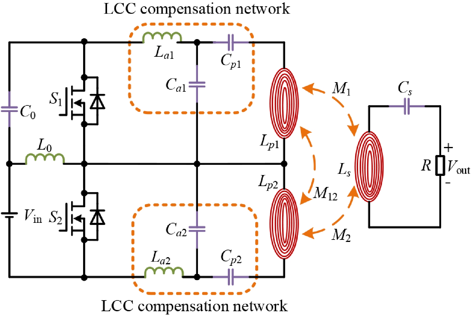
Figure 3.
Main circuit of the proposed dual-output inverter with wide soft-switching range for dynamic wireless charging of electric vehicles.
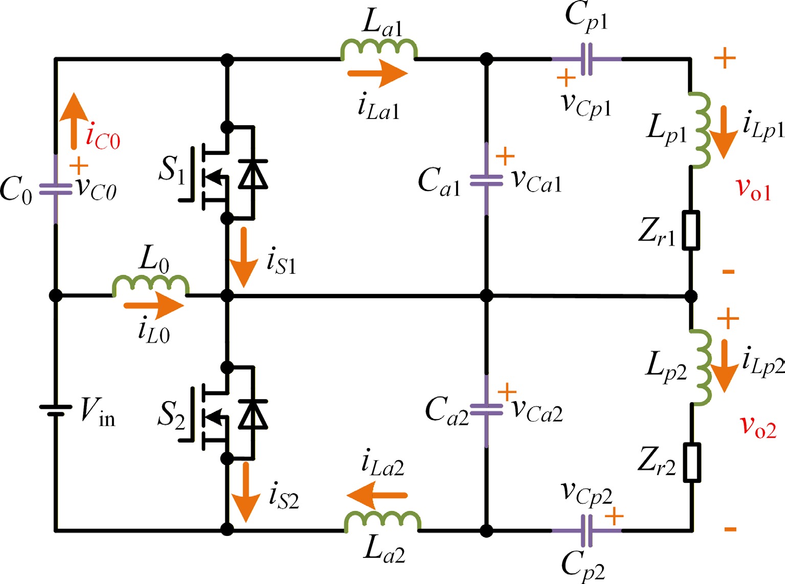
Figure 4.
Equivalent circuit of Fig. 3.
Operating principle
-
To analyze the operating principle of the proposed inverter, the following assumptions are made: (1) Inductors and capacitors are ideal components with no internal resistance, and C0 is sufficiently large to maintain a constant voltage across its terminals; (2) The internal resistance and voltage drop of all switches are equal to zero; (3) The parameters of each energy transmitter are symmetrical. The relevant parameters can be expressed as follows:
$ \left\{ {\begin{array}{*{20}{l}} {{L_{a{\text{1}}}}{\text{ = }}{L_{a2}}{\text{ = }}{L_a}} \\ {{C_{a{\text{1}}}}{\text{ = }}{C_{a2}}{\text{ = }}{C_a}} \\ {{C_{p{\text{1}}}}{\text{ = }}{C_{p2}}{\text{ = }}{C_p}} \\ {{L_{p{\text{1}}}}{\text{ = }}{L_{p2}}{\text{ = }}{L_p}} \end{array}} \right. $ (1) Considering the influence of cross-mutual inductance, the expressions of the system resonant angular frequency ω0 and resonant frequency f0 are as follows:
$ {\omega _0}{\text{ = }}2\pi {f_0}{\text{ = }}\dfrac{1}{{\sqrt {{L_a}{C_a}} }}{\text{ = }}\dfrac{1}{{\sqrt {\left( {{L_p} + {M_{12}} - {L_a}} \right){C_p}} }}{\text{ = }}\dfrac{1}{{\sqrt {{L_s}{C_s}} }} $ (2) where, fS denotes the switching frequency of the proposed inverter and f0 denotes the resonant frequency of the system.
When fS is equal to f0, the key operating waveforms of the inverter are illustrated in Fig. 5, where T and D are the operating period and duty cycle of the inverter, respectively. td denotes the dead zone to prevent the bridge arm from passing through; VB is the amplitude of the inverter's input voltage. The expression defining VB is:
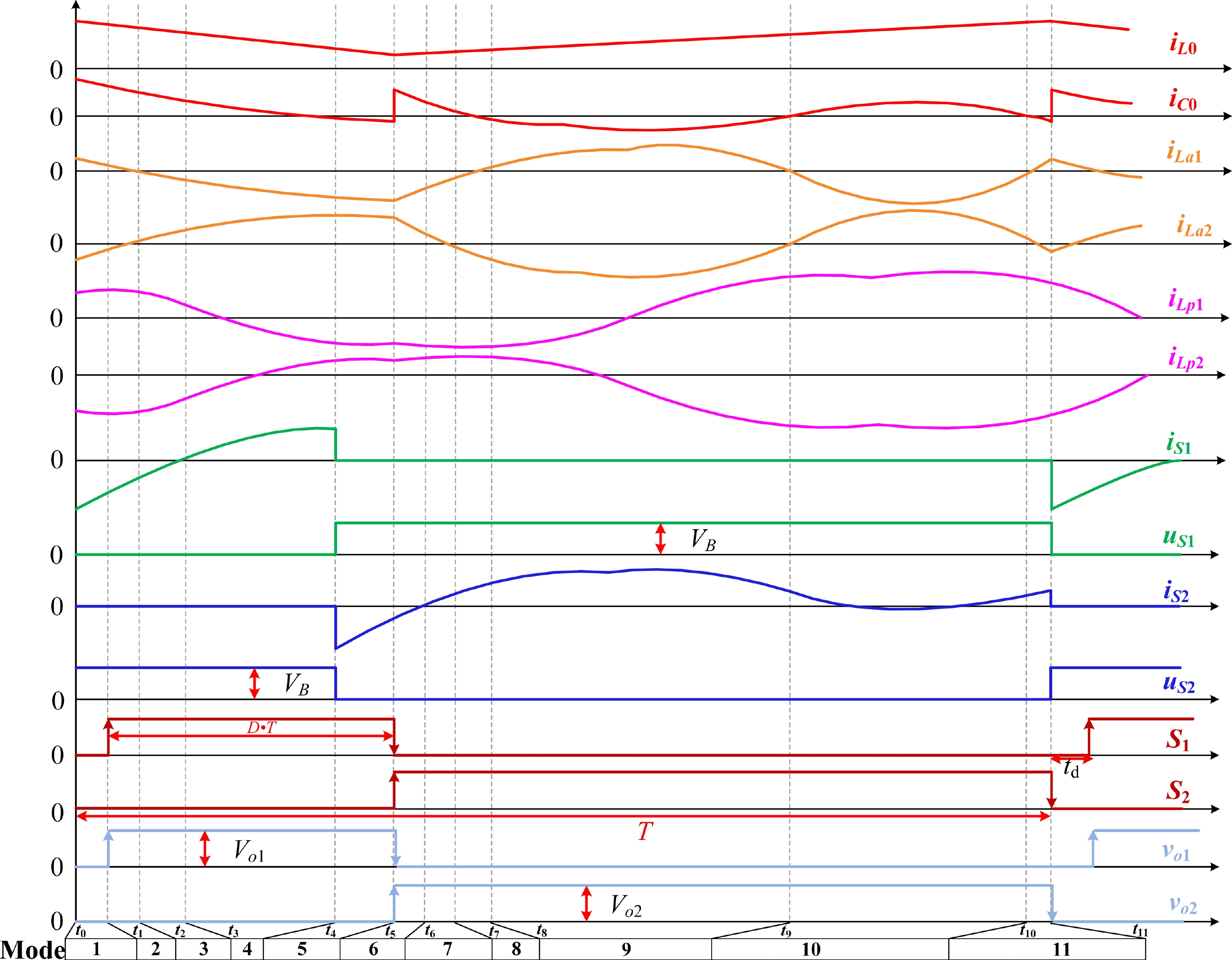
Figure 5.
Theoretical operating waveforms of key components.
$ {V_B}{\text{ = }}{V_{C0}} + {V_{{\text{in}}}} $ (3) The equivalent circuits of the inverter for various operating modes are illustrated in Fig. 6, where the directions marked by each arrow are the actual directions of each current at the initial instant of the mode. The proposed inverter has 11 operating modes in one operating cycle, and the analysis of each operating mode is as follows:
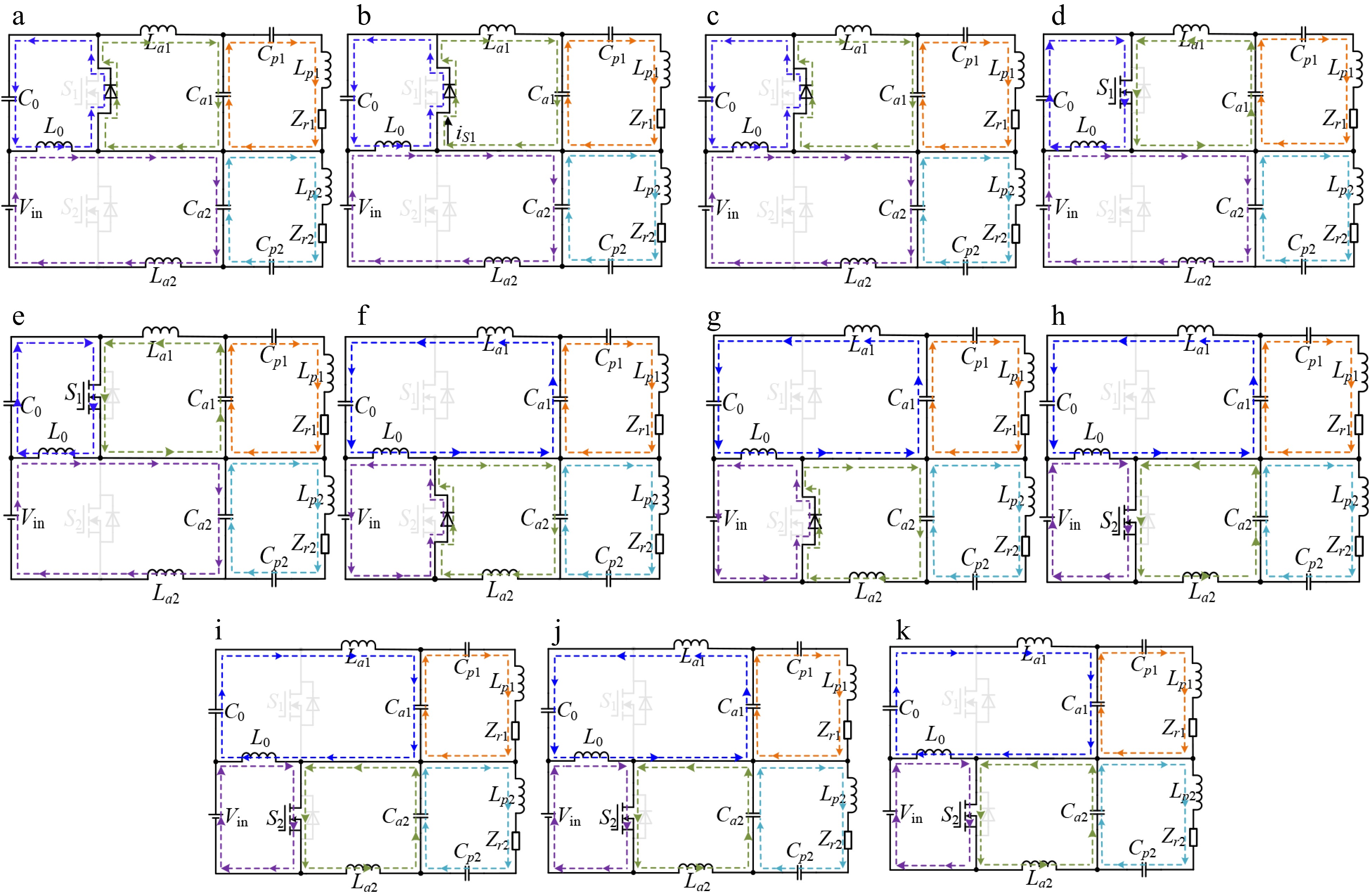
Figure 6.
Equivalent circuits in each of the operating modes. (a) Mode 1; (b) Mode 2; (c) Mode 3; (d) Mode 4; (e) Mode 5; (f) Mode 6; (g) Mode 7; (h) Mode 8; (i) Mode 9; (j) Mode 10; (k) Mode 11.
(1) Mode 1 (t0~t1): At t0, S2 is turned off. The current iS2 flowing through S2 is commutated to S1 and flows through its body diode, denoted as iS1. Meanwhile, vo1 decreases to zero while vo2 increases to VB. iC0 reverses polarity and C0 enters charging state. In this mode, iL0 starts to decrease linearly from its maximum value.
(2) Mode 2 (t1~t2): At t1, S1 is turned on. When S1 is turned on, the voltage stress across S1 is zero, enabling S1 to achieve ZVS turn-on. In this mode, iL0 continues to decrease linearly. Simultaneously, the condition for S1 to achieve ZVS turn-on is derived as follows:
$ {i_{S2}}\left( {{t_0}} \right) \gt 0 $ (4) If Eq. (4) is not satisfied, when S2 is turned off, uS2 is clamped to zero by its body diode, enabling ZVS turn-off of S2.
(3) Mode 3 (t2~t3): At t2, iLa1 crosses zero in the reverse direction, and iLa2 crosses zero in the forward direction; subsequently, iLa1 starts to increase in the reverse direction, while iLa2 starts to increase in the positive direction. In this mode, iL0 continues to decrease linearly.
(4) Mode 4 (t3~t4): At t3, iS1 crosses zero in the positive direction, commutates from the body diode of S1 to S1 itself, and S1 begins to conduct. In this mode, iL0 continues to decrease linearly.
(5) Mode 5 (t4~t5): At t4, iC0 crosses zero in the reverse direction, and C0 enters the state. In this mode, iL0 continues to decrease linearly.
(6) Mode 6 (t5~t6): At t5, S1 is turned off. iS1 is commutated to S2 and flows through its body diode. vo2 drops to zero while vo1 rises to VB. iC0 reverses polarity and C0 enters a charging state. In this mode, iL0 starts to increase linearly from its minimum value.
(7) Mode 7 (t6~t7):At t6, S2 is turned off. Since the voltage stress across S2 is zero at turn on, S2 can achieve ZVS turn on. In this mode, iL0 continues to increase linearly. Meanwhile, the condition for S2 to achieve ZVS turn-on is derived as follows:
$ {i_{S1}}\left( {{t_5}} \right) \gt 0 $ (5) If Eq. (5) is not satisfied, when S1 is turned off, uS1 is clamped to zero by the body diode of S1, enabling ZVS turn-off of S1.
(8) Mode 8 (t7~t8): At t7, iS2 crosses zero, iS2 transfers from the body diode of S2 to S2, and S2 begins to conduct. In this mode, iL0 continues to rise linearly.
(9) Mode 9 (t8~t9): At t8, iC0 and iLa2 cross zero in the reverse direction, iLa1 crosses zero in the forward direction, and C0 enters a discharging state. In this mode, iL0 continues to increase linearly.
(10) Mode 10 (t9~t10): At t9, iC0 and iLa2 cross zero in the forward direction, iLa1 crosses zero in the reverse direction, and C0 enters a charging state. In this mode, iL0 continues to increase linearly.
(11) Mode 11 (t10~t11): At t10, iC0 and iLa2 cross zero in the reverse direction again, iLa1 crosses zero in the forward direction again, and C0 enters a discharging state again. In this mode, iL0 continues to increase linearly. At t11, S2 is turned off and the inverter enters the next operating cycle.
-
With regard to Fig. 5, the dead time td is much smaller than the inverter′s duty cycle T and can be ignored to simplify the analysis. Based on the operating principle of the dual-output inverter, the voltage expression across L0 is derived as:
$ {V_{L0}}{\text{ = }}\left\{ \begin{array}{*{20}{l}} - {V_{C{\text{0}}}}&{{t_0} \leqslant t \leqslant {t_5}} \\ {V_{{\text{in}}}}&{{t_5} \leqslant t \leqslant T} \end{array} \right. $ (6) In steady state, the volt-second balance theorem is applied to inductor L0, leading to the following equation:
$ {V_{{\text{in}}}}DT = {V_{C0}}\left( {1 - D} \right)T $ (7) Combining Eqs (3) and (7), the expressions for VC0 and VB are derived as follows:
$ {V_{C0}}{\text{ = }}\dfrac{{D{V_{{\text{in}}}}}}{{1 - D}} $ (8) $ {V_B}{\text{ = }}\dfrac{{{V_{{\text{in}}}}}}{{1 - D}} $ (9) According to Fig. 5, the Fourier series expansions of the two output voltages vo1 and vo2 of the inverter are obtained by ignoring the dead time.
$ {v_{o1}} = D{V_B} - \dfrac{{\sqrt 2 {V_B}}}{\pi }\sum\limits_{n = 1}^\infty {\left[ {\dfrac{{\sqrt {1 - \cos 2n\pi D} }}{n}\sin \left( {n{\omega _0}t - {\varphi _n}} \right)} \right]} $ (10) $ {v_{o2}} = \left( {1 - D} \right){V_B} + \dfrac{{\sqrt 2 {V_B}}}{\pi }\sum\limits_{n = 1}^\infty {\left[ {\dfrac{{\sqrt {1 - \cos 2n\pi D} }}{n}\sin \left( {n{\omega _0}t - {\varphi _n}} \right)} \right]} $ (11) φn = arctan [cot (nπD)] denotes the phase of the nth harmonic of vo1 and vo2.
The phasor expression for the RMS value of the nth harmonic of vo1 and vo2 is as follows:
$ \left\{ {\begin{array}{*{20}{l}} {{{\dot V}_{o1n}} = {V_{o1n}}\angle {\varphi _n} = \dfrac{{{V_B}\sqrt {1 - \cos \left( {2n\pi D} \right)} }}{{n\pi }}\angle \left( {\pi - {\varphi _n}} \right)} \\ {{{\dot V}_{o2n}} = {V_{o2n}}\angle {\varphi _n} = \dfrac{{{V_B}\sqrt {1 - \cos \left( {2n\pi D} \right)} }}{{n\pi }}\angle - {\varphi _n}} \end{array}} \right. $ (12) It can be seen from Eq. (12) that the two output voltages of the dual-output inverter are equal in magnitude and opposite in direction. Since the LCC network has excellent filtering characteristics, the rail current approximates a sine wave, with energy primarily transmitted through the fundamental component. The inverter's output voltage gain is defined as:
$ {M_{v - p}} = \dfrac{{\left| {{{\dot V}_{o1,1}}} \right|}}{{{V_{{\text{in}}}}}} = \dfrac{{\left| {{{\dot V}_{o2,1}}} \right|}}{{{V_{{\text{in}}}}}} $ (13) where,
$ \left| {{{\dot V}_{o1,1}}} \right| $ $ \left| {{{\dot V}_{o2,1}}} \right| $ The relationship between Mv-p and D is depicted in Fig. 7. In practical operation, when D = 1, iL0 will increase continuously, eventually resulting in excessive current through the inverter, which may lead to burnout. To ensure an adequate safety margin for the inverter, the range of D in Fig. 7 is set to 0~0.9. It can be seen from Fig. 7 that Mv-p is positively correlated with D, with Mv-p|D=0.5 = 0.9003,and Mv-pmax = 1.391.
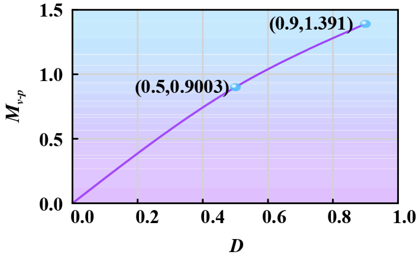
Figure 7.
The relationship between Mv-p and D.
Comparative analysis
-
Table 1 compares the proposed dual-output inverter with existing common inverters in terms of output voltage gain range, number of input and output ports, and the number of switching devices. From Table 1, it is evident that the proposed dual-output inverter offers a wider voltage gain range compared to existing inverters. In terms of output quantity, all inverters except the three-phase inverter are single-output. However, the three-phase inverter requires three times as many switching devices as the proposed dual-output inverter, and there exists a phase difference between its phase outputs. Regarding the number of switching devices, both the voltage-type half-bridge inverter and the proposed dual-output inverter require only two switching devices. However, the voltage-type half-bridge inverter has a lower output voltage gain and fewer outputs compared to the proposed dual-output inverter. In summary, the proposed dual-output inverter can achieve more outputs and a wider voltage gain range with fewer switching devices, enabling synchronous driving of more transmitter coils.
Table 1. The comparison between the proposed dual output inverter and several typical inverters.
Type of inverter Voltage gain Number of input ports Number of output ports Number of switching devices Voltage type half bridge inverter 0~0.45 1 1 2 Voltage type full bridge inverter 0~0.9 1 1 4 Matrix converter 0~0.64 1 1 8 Multi-level inverter 0~1.35 1 1 8 Three-phase inverter 0~0.78 1 3 6 The proposed inverter 0~1.39 1 2 2 Output power analysis of the power system
-
Using the fundamental equivalence principle, Fig. 3 can be simplified to the equivalent circuit shown in Fig. 8. In Fig. 3, the phases of iLa2 and iLp2 are opposite to those of iLa1 and iLp1. Thus, in practical applications, the connection direction of the inverter's second output network should be reversed to ensure that iLa1 and iLa2, as well as iLp1 and iLp2, are in phase, thereby avoiding power imbalance. Therefore, for ease of analysis in this section, iLp1 and iLp2 are reversed in phase.
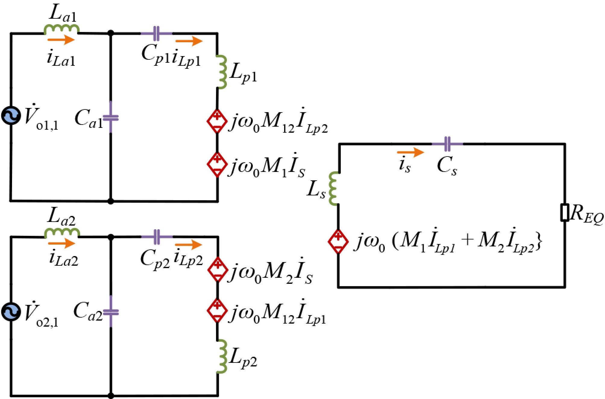
Figure 8.
The mutual inductance equivalent circuit in Fig. 3.
Based on Kirchhoff's law of voltage (KVL), the relationship between system voltage and current is expressed as follows:
$ \left[ {\begin{array}{*{20}{c}} {{{\dot V}_{o1,1}}} \\ {{{\dot V}_{o2,1}}} \\ {{{\dot V}_{o1,1}}} \\ {{{\dot V}_{o2,1}}} \\ 0 \end{array}} \right]{\text{ = }}\left[ \begin{array}{*{20}{c}} {{Z_a}} &{ - {1 / {j{\omega _0}{C_a}}}} & 0 & 0 & 0 \\ 0 & 0& {{Z_a}} & { - {1 /{j{\omega _0}{C_a}}}} & 0 \\ {j{\omega _0}{L_a}}&{{Z_p}} & 0 & 0 &-{j{\omega _0}{M_1}} \\ 0 &0 & {j{\omega _0}{L_a}} & {{Z_p}}&-{j{\omega _0}{M_2}} \\ 0&{ j{\omega _0}{M_1}} & 0 &{ j{\omega _0}{M_2}} &{ - {Z_s} - R} \end{array} \right] \left[ {\begin{array}{*{20}{c}} {{{\dot I}_{La1}}} \\ {{{\dot I}_{Lp1}}} \\ {{{\dot I}_{La2}}} \\ {{{\dot I}_{Lp2}}} \\ {{{\dot I}_s}} \end{array}} \right] $ (14) where,
$ \left\{ {\begin{array}{*{20}{l}} {{Z_a} = j{\omega _0}{L_a} + \dfrac{1}{{j{\omega _0}{C_a}}}} \\ {{Z_p} = j{\omega _0}\left( {{L_p} + {M_{12}}} \right) + \dfrac{1}{{j{\omega _0}{C_p}}}} \\ {{Z_s} = j{\omega _0}{L_s} + \dfrac{1}{{j{\omega _0}{C_s}}}} \end{array}} \right. $ By substituting Eqs (2) and (14) into Eq. (13), the expression of current in each branch of the system can be obtained as:
$ \left\{ {\begin{array}{*{20}{l}} {{{\dot I}_{L1}} = \dfrac{{{{\dot V}_{o1,1}}{M_1}\left( {{M_1} + {M_2}} \right)}}{{{L_a}^2R}}} \\ {{{\dot I}_{L2}} = \dfrac{{{{\dot V}_{o1,1}}{M_2}\left( {{M_1} + {M_2}} \right)}}{{{L_a}^2R}}} \\ {{{\dot I}_{p1}} = \dfrac{{{{\dot V}_{o1,1}}}}{{j{\omega _0}{L_a}}}} \\ {{{\dot I}_{p2}} = \dfrac{{{{\dot V}_{o1,1}}}}{{j{\omega _0}{L_a}}}} \\ {{{\dot I}_s} = \dfrac{{{{\dot V}_{o1,1}}\left( {{M_1} + {M_2}} \right)}}{{{L_a}R}}} \end{array}} \right. $ (15) From Eq. (15), it can be observed that İp1and İp2 are equal in magnitude and phase, and are independent of R, M1, and M2. Thus, two high-frequency currents with the same phase and magnitude can be generated in the two transmitting coils, avoiding complicated phase synchronization control. Based on Eq. (15), the system output power expression is further derived as:
$ {P}_{out}={\left|{\dot{I}}_{s}\right|}^{2}\cdot R=\dfrac{{V}_{o1,1}^{2}{\left({M}_{1}+{M}_{2}\right)}^{2}}{{L}_{a}{}^{2}R} $ (16) Using the parameters in Table 2 as the main parameters, the system output power characteristic curves are depicted in Fig. 9. Figure 9a illustrates the relationship between output power Pout, duty cycle D and mutual inductance M1 + M2. It can be seen that in the resonance state, Pout is positively correlated with D and M1 + M2. Figure 9b depicts the relationship between Pout, M1, and M2 at D = 0.5. It can be seen that Pout is positively correlated with M1 and M2, and the influence of M1 and M2 on Pout is symmetrical.
Table 2. Main system parameters.
Parameter Value Parameter Value Vin 100 V La 50 μF Lp 100 μH Ca 70.12 nF L0 150 μH Cp 62.94 nF Ls 130 μH R 5 Ω C0 100 μF M12 5.7 μH Cs 26.97 nF f0 85 kHz 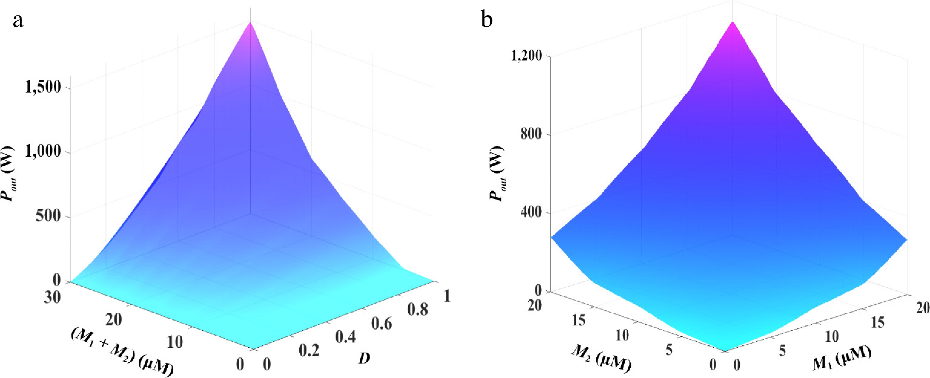
Figure 9.
The relationship among Pout with D, M1, and M2. (a) The relationship among Pout with D and M1 + M2. (b) The relationship among Pout with M1 and M2.
Operating conditions of soft-switching
-
According to Fig. 5, the voltage stress of S1 and S2 is:
$ {v_{S1\max }} = {v_{S2\max }} = {V_B} $ (17) The current stress on S1 and S2 is expressed as:
$ {i_{S1\max }} = {i_{S2\max }} = {i_{S2}}\left( {{t_0}} \right) $ (18) According to Figs. 5 and 6, the following expressions are derived:
$ {i_{S1}} = \left\{ {\begin{array}{*{20}{l}} {i_{L2}} - {i_{L1}} - {i_{L0}}&{{t_0} \leqslant t \leqslant {t_5}} \\ 0&{{t_5} \leqslant t \leqslant {t_{11}}} \end{array}} \right. $ (19) $ {i_{S2}} = \left\{ {\begin{array}{*{20}{l}} 0&{{t_0} \leqslant t \leqslant {t_5}} \\ {i_{L0}} + {i_{L1}} - {i_{L2}}&{{t_5} \leqslant t \leqslant {t_{11}}} \end{array}} \right. $ (20) According to Eqs (10) and (15), the fundamental wave time domain expressions of iLa1 and iLa2 are obtained as follows:
$ \left\{ {\begin{array}{*{20}{l}} {{i_{La1,1}}\left( t \right) = \sqrt 2 \left| {{{\dot I}_{La1}}} \right|\sin \left( {{\omega _0}t + \pi - {\phi _1}} \right)} \\ {{i_{La2,1}}\left( t \right) = \sqrt 2 \left| {{{\dot I}_{La2}}} \right|\sin \left( {{\omega _0}t - {\phi _1}} \right)} \end{array}} \right. $ (21) where, iLa1,1(t) and iLa2,1(t) represent the fundamental components extracted from the Fourier series expansions of iLa1 and iLa2, respectively.
To enhance analysis accuracy, it is necessary to calculate the higher harmonics of iLa1 and iLa2. According to[28], the LCC network can be simplified as shown in Fig. 10 under high-order harmonics. It can be observed that high-order harmonics almost all the high-frequency current flows through La and Ca, while the transmitting coil circuit is equivalent to an open circuit. This explains why iLa1 and iLa2 exhibit high distortion,whereas iLp1 and iLp2 have high sinusoidality in Fig. 5.
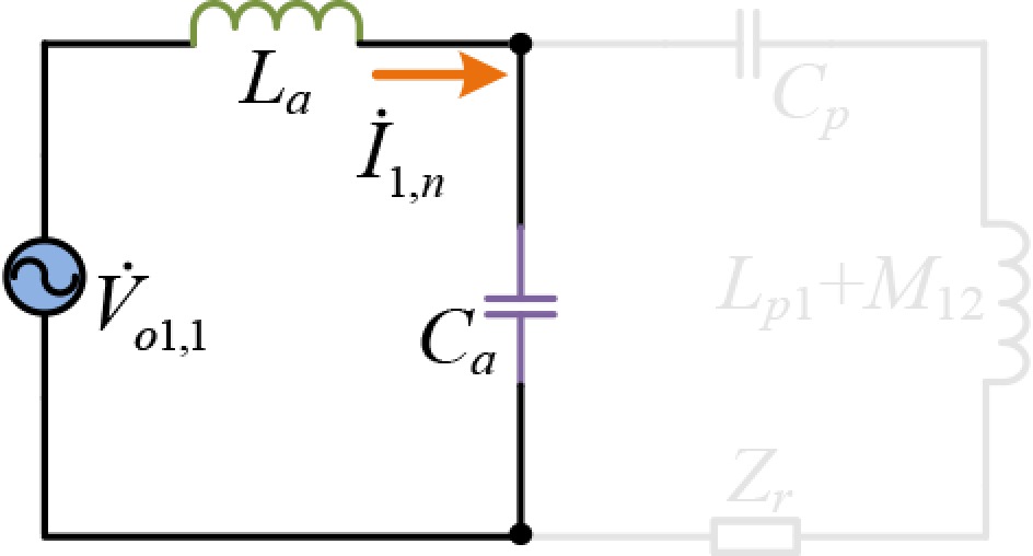
Figure 10.
Simplified model of LCC network under high order harmonics.
According to Fig. 10, the impedance expression of LCC network under the nth harmonic is as follows:
$ {Z_{1,n}} = jn{\omega _0}{L_a} + \dfrac{1}{{jn{\omega _0}{C_a}}} = j{Z_a}\dfrac{{{n^2} - 1}}{n} $ (22) where,
$ {Z_a} = {\omega _0}{L_a} = \sqrt {{{{L_a}} \mathord{\left/ {\vphantom {{{L_a}} {{C_a}}}} \right. } {{C_a}}}} ,\begin{array}{*{20}{c}} {}&{n \geqslant 2} \end{array} $ Hence, the nth harmonic expressions of iLa1 and iLa2 are obtained:
$ \left\{ {\begin{array}{*{20}{l}} {{i_{La1,n}}\left( t \right) = \sqrt 2 \dfrac{{\left| {{{\dot V}_{o1,n}}} \right|}}{{\left| {{Z_{1,n}}} \right|}}\sin \left( {n{\omega _0}t - {\phi _n} + \dfrac{\pi }{2}} \right)} \\ {{i_{La2,n}}\left( t \right) = \sqrt 2 \dfrac{{\left| {{{\dot V}_{o2,n}}} \right|}}{{\left| {{Z_{1,n}}} \right|}}\sin \left( {n{\omega _0}t - {\phi _n} + \dfrac{\pi }{2}} \right)} \end{array}} \right. $ (23) Then the total expression of iLa1 and iLa2 is as follows:
$ \left\{ {\begin{array}{*{20}{l}} {{i_{La1}}\left( t \right) = {i_{La1,1}}\left( t \right) + \sum\limits_{n = 2}^\infty {{i_{La1,n}}\left( t \right)} } \\ {{i_{La2}}\left( t \right) = {i_{La1,1}}\left( t \right) + \sum\limits_{n = 2}^\infty {{i_{La1,n}}\left( t \right)} } \end{array}} \right. $ (24) Assuming ideal system operation (with zero losses), the average value of the inverter input current iin can be expressed using the law of energy conservation as:
$ {i_{{\text{in}}}} = {i_{L0m}} - {i_{C0m}} = \dfrac{{{P_{out}}}}{{{V_{{\text{in}}}}}} $ (25) where, iL0m denotes the average value of iL0, and iC0m denotes the average value of iC0. In steady state, the capacitor satisfies the ampere-second balance principle, that is iC0m = 0, then Eq. (25) can be rewritten as:
$ {i_{L0m}} = \dfrac{{{P_{out}}}}{{{V_{{\text{in}}}}}} $ (26) When S2 is turned on, iL0 increases linearly, so the fluctuating value expression of iL0 is as follow:
$ \Delta {i_{L0}} = \dfrac{{{V_{{\text{in}}}}DT}}{{{L_0}}} $ (27) The expressions of iS2 and iS1 when the switches turn on are as follows:
$ \left\{ {\begin{array}{*{20}{l}} {{i_{S2}}\left( {{t_0}} \right) = {i_{L0m}} + \dfrac{{\Delta {i_L}}}{2} + {i_{La1}}\left( {{t_0}} \right) - {i_{La2}}\left( {{t_0}} \right)} \\ {{i_{S1}}\left( {{t_5}} \right) = {i_{La2}}\left( {{t_5}} \right) - {i_{La1}}\left( {{t_5}} \right) - {i_{L0m}} + \dfrac{{\Delta {i_L}}}{2}} \end{array}} \right. $ (28) According to Eq. (28), the current stress of the switching devices and the soft-switching operating states can be determined. Using the parameters in Table 2 as the main system parameters, the relationship between iS2(t0) with D, M1, and M2 is depicted in Fig. 11a. Figure 11b is a cross-sectional view of Fig. 11a at M2 = 15 μH. It can be observed that iS2(t0) is always positive regardless of the values of M1, M2, and D, indicating that ZVS turn on of S1 can be achieved at any position of the receiving coil. The larger M1, M2, and D, the greater iS2(t0) and the lower the current stress on the switches. Figure 12 illustrates the relationship between iS1(t5), D, M1, and M2. Figure 12a shows the influence of M1 and M2 values on iS1(t5) under different duty cycles, while Fig. 12b presents the polarity boundary of iS1(t5) in Fig. 12a. It can be observed that for a fixed duty cycle, the larger M1 + M2, the closer the receiving coil is to the center of the transmitting coil, the easier it is to achieve ZVS turn-off of S1. Furthermore, the smaller M1 + M2, the closer the pick-up coil is to the edge of the transmitting coils, the easier it is to achieve ZVS turn-on of S2. In any case, the inverter can always achieve two soft-switching states, which can reduce switching losses.
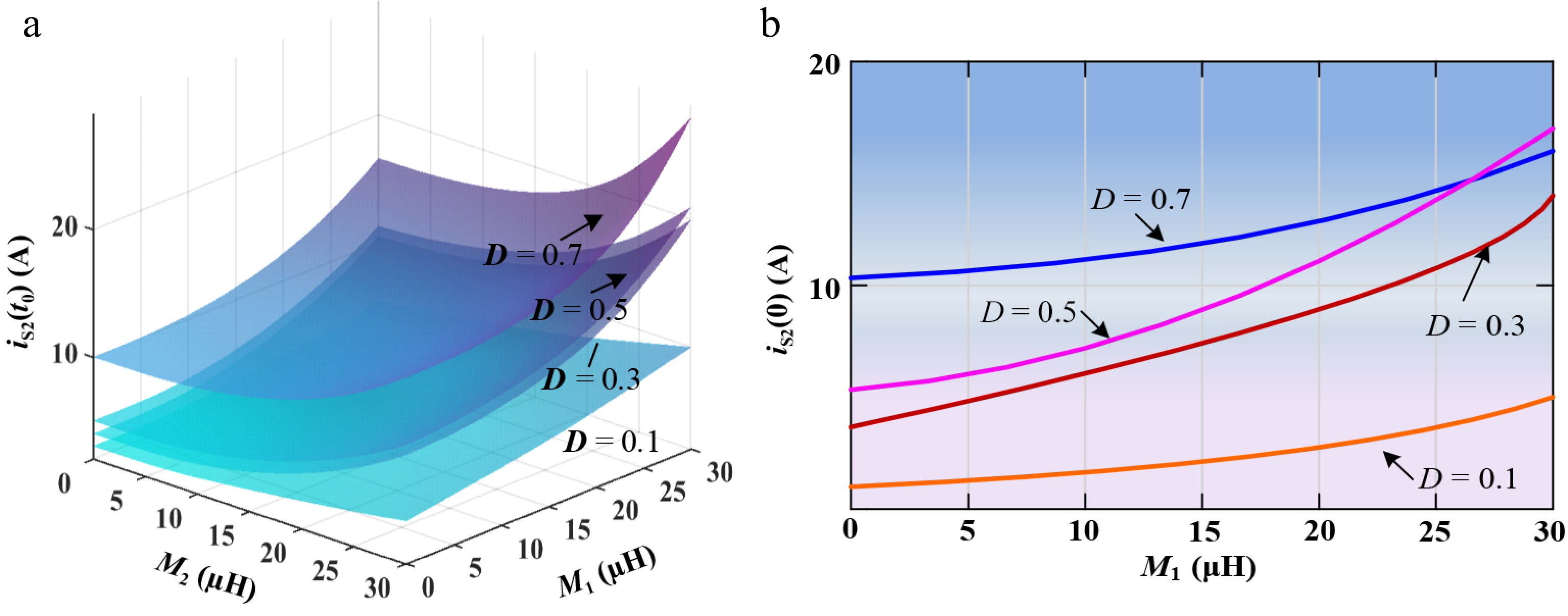
Figure 11.
The relationship among iS2(t0) with D, M1, and M2. (a) The relationship among iS2(t0) with D, M1, and M2 under different duty cycle conditions; (b) Cross-sectional view of (a) when M2 = 15 μH.
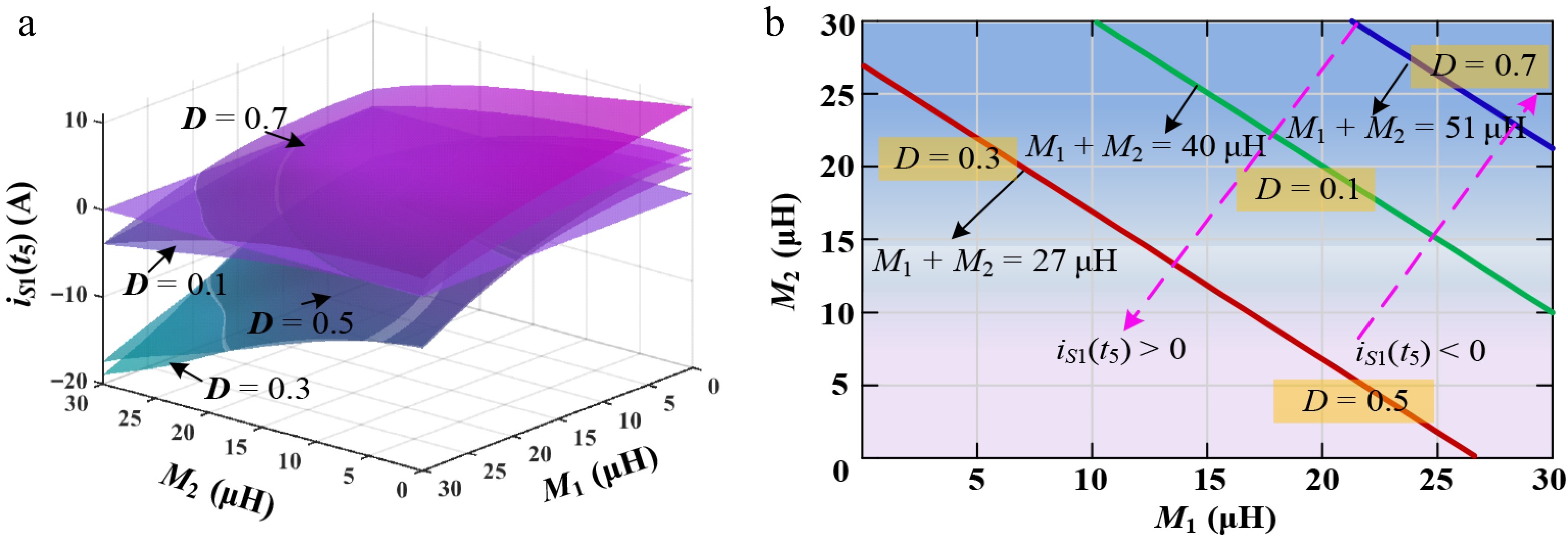
Figure 12.
The relationship among iS1(t5) with D, M1, and M2. (a) The relationship among iS1(t5) with D, M1, and M2 under different duty cycle conditions; (b) Polarity boundary line of iS1(t5).
-
To verify the correctness of the theoretical analysis, and the feasibility and superiority of the proposed dual-output inverter, an experimental platform was built as shown in Fig. 13 according to the parameters in Table 2. The experimental setup consists of a DSP and FPGA controller, a dual-output inverter, a resonant compensation network, a coupling mechanism, and a load resistor. The DSP controller is used to generate drive signals for S1 and S2. The schematic diagram of the coupling mechanism is shown in Fig. 14a. The position x = 0 is defined as the receiver coil being centered between the two transmitter coils. The measured values of mutual inductances M1, M2, and M12 as functions of x are shown in Fig. 14b. It can be seen from Fig. 14b that M1 and M2 reach their maximum values at x = −7.5cm and x = 7.5 cm respectively. M1 + M2 is approximately symmetric with respect to x = 0, while M12 remains nearly constant.
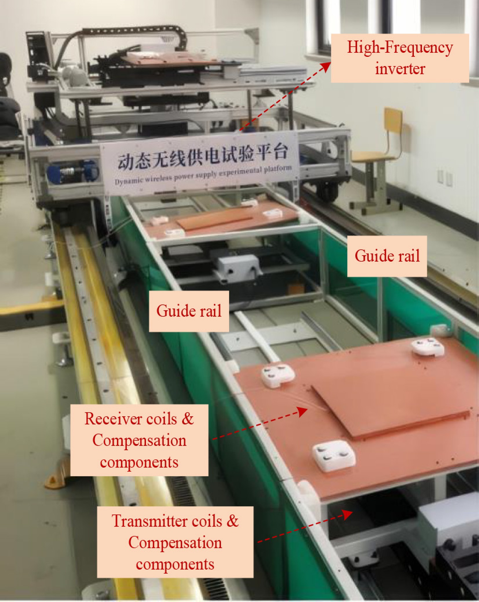
Figure 13.
Experimental platform.
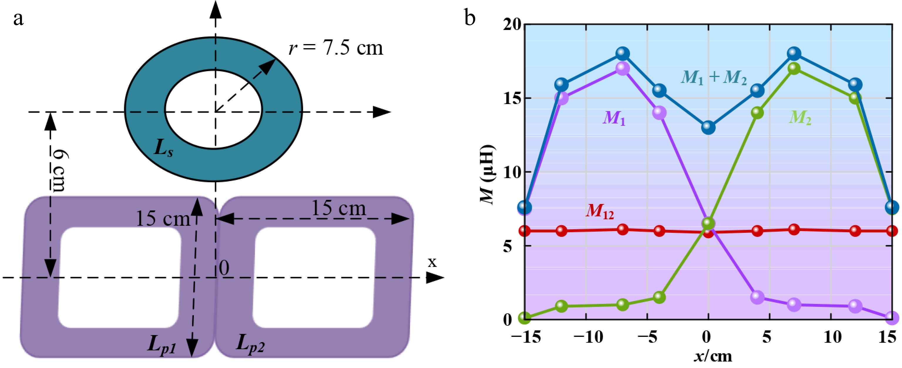
Figure 14.
The magnetic coupler. (a) Schematic diagram; (b) Measured mutual inductances vary with x-axis.
Steady-state characteristic test
-
Figure 15 shows the experimental waveforms of the inverter output voltage and transmitting coil current at x = 0 and 7.5 cm, D = 0.3 and D = 0.7. It can be seen from Fig. 15 that when D = 0.3 and 0.7, the experimental values of VB are 140 and 330 V, respectively. Meanwhile, the amplitudes and phases of iLp1 and iLp2 are essentially the same; the slight discrepancy arises primarily from the fact that the parameters of the two output resonant compensation networks of the inverter are not strictly consistent in practice. With the increasing D, the effective values of rail current are approximately 2 and 4.4 A, respectively. Using Eqs (10) and (15), the inverter output voltage gains are calculated to be 0.534 and 1.175, verifying the voltage output capability of the dual-output inverter.
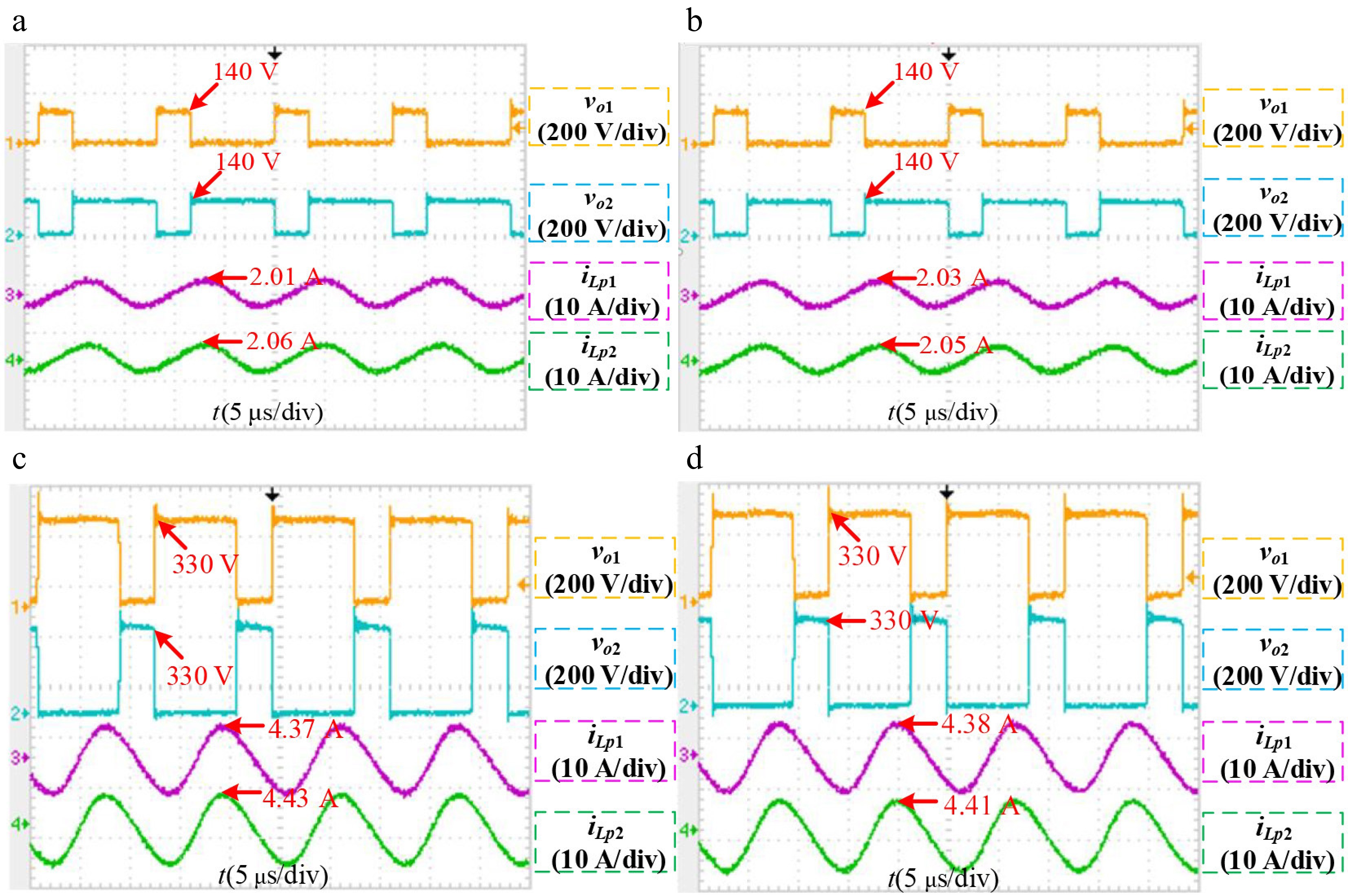
Figure 15.
Experimental waveforms of the inverter output voltages and primary coil currents. (a) x = 0, D = 0.3; (b) x = 7.5, D = 0.3; (c) x = 0, D = 0.7; (d) x = 7.5, D = 0.7.
Figure 16 shows the switching waveforms of S1 and S2 at x = 7.5, D = 0.3; x = 0, D = 0.3; x = 7.5, D = 0.7; and x = 0, D = 0.7. vS1 and vS2 are the terminal voltages of S1 and S2 respectively. Taking x = 7.5 cm, D = 0.3 as an example: At t0, S1 is turned off and the drive voltage begins to decrease. At t1, S2 is turned on and the drive voltage starts to rise; prior to this, vS2 has dropped to zero, indicating that S2 achieves ZVS turn-on. At t2, S2 is turned off and the drive voltage begins to decrease. At t3, S1 is turned on and the drive voltage begins to rise. Before that, vS1 has dropped to zero, indicating that S1 achieves ZVS turn-on. Further analysis confirms that S1 and S2 achieve ZVS turn-on in all other waveforms. Combined with Figs. 11 and 14b, these results demonstrate that S1 and S2 can achieve ZVS turn-on under different duty cycles throughout the movement of the receiver coil from transmitting rail 1 to transmitting rail 2.
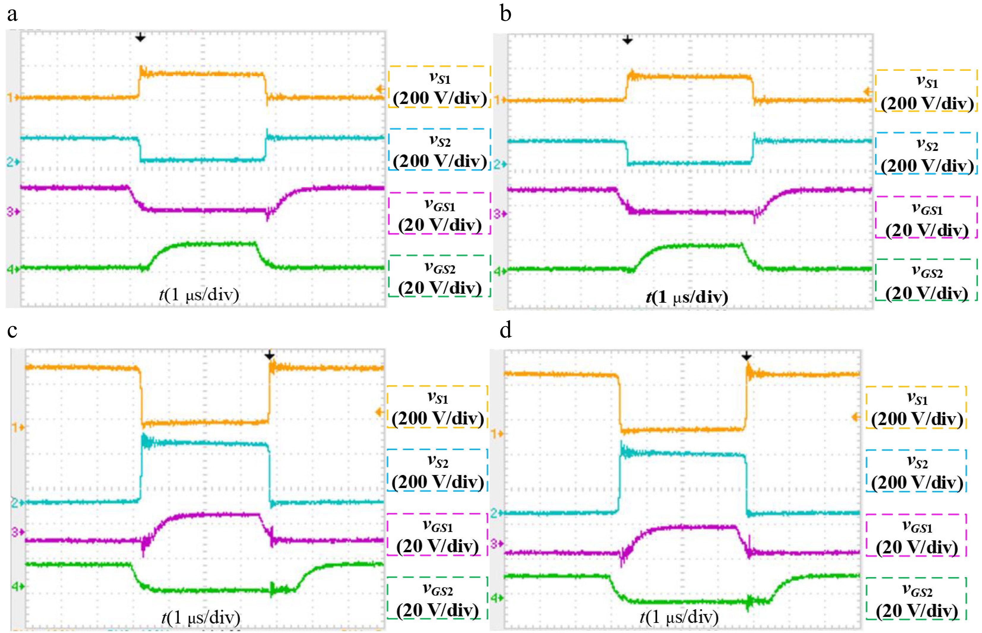
Figure 16.
Experimental waveforms of two switches. (a) x = 7.5, D = 0.3; (b) x = 0, D = 0.3; (c) x = 7.5, D = 0.7; (d) x = 0, D = 0.7.
Figure 17 shows the characteristic curves of system output power Pout and efficiency η. It can be seen that Pout fluctuates to some extent as the receiving coil moves, with larger fluctuations occurring at higher D values. Pout reaches its maximum when the receiving coil is directly aligned with each transmitting rail (x = −7.5 cm and x = 7.5 cm). According to Eq. (16) and Fig. 9, when La and R are constant, Pout is positively correlated with M1 + M2 for a given D. As shown in Fig. 14, M1 + M2 and Pout reach their maximum values at x = −7.5 cm and x = 7.5 cm, which is consistent with the theoretical analysis. The efficiency curve shows that η also fluctuates with the movement of the receiving coil, and at the same x, η decreases slightly with increasing D. Overall, the system maintains high transmission efficiency across different x and D values, with a maximum efficiency exceeding 90%.
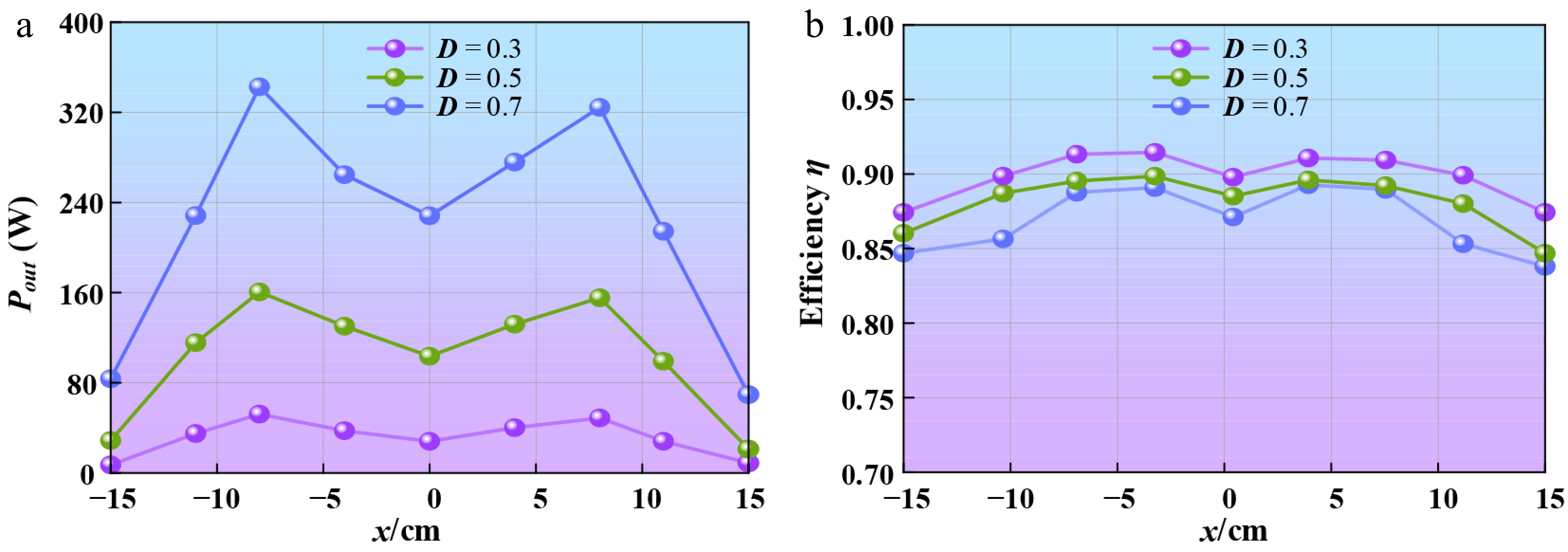
Figure 17.
Curves of the system output power and efficiency. (a) Output power; (b) Transfer efficiency.
Dynamic characteristic test
-
Figure 18 shows the load change waveform of the system at D = 0.5 and x = −7.5 cm. It can be seen that when the load changes, all parameters remain stable except for iL0, which adjusts accordingly. The spike oscillation in Vout during load changes is attributed to the mechanical switch used to adjust the resistance, which introduces transient oscillations and noise during switching, affecting the Vout waveform. As observed, the system response time to load changes is only a few milliseconds, indicating a fast dynamic response.
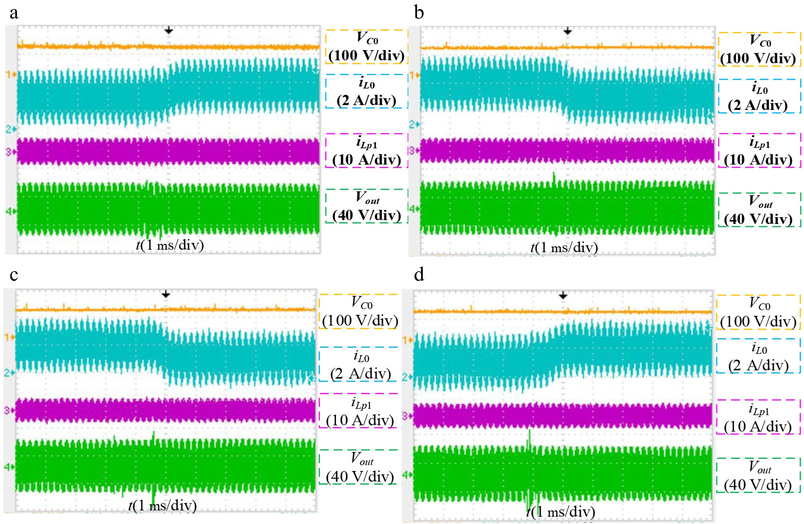
Figure 18.
Experimental waveforms of VC0, iL0, iLp1, and Vout under load change: (a) 5 to 3.3 Ω; (b) 3.3 to 5 Ω; (c) 5 to 10 Ω; (d) 10 to 5 Ω.
-
The proposed high-frequency dual-output inverter represents a significant advancement in the field of dynamic WPT for electric vehicles. By generating two identical output voltages to synchronously the transmitter coils, it effectively reduces the number of inverters and simplifies system control, addressing a long-standing challenge in multi-coil WPT systems. The wide output voltage gain range ensures sufficient voltage output capacity while minimizing the number of switches, reducing both hardware costs and overall system complexity. The ZVS feature of the inverter is another crucial advantage, as it significantly mitigates switching losses, thereby enhancing the overall efficiency of the WPT system.
The experimental results further validate the effectiveness of the proposed inverter. The WPT system demonstrates remarkable performance, maintaining high transmission efficiency across different positions of the receiver coil. With a maximum efficiency exceeding 90% and a minimum of around 85%, it outperforms many existing solutions. Additionally, the fast dynamic response speed ensures stable power transfer even under varying conditions. However, this research has limitations: the suppression of output power fluctuations, a critical issue in dynamic WPT systems, has not been fully addressed. Future research will focus on developing effective suppression technologies to enhance the stability of electric vehicle dynamic wireless charging systems, promoting the practical application and widespread adoption of this promising technology.
-
A high-frequency dual-output inverter with wide soft-switching range for dynamic WPT of electric vehicles is proposed. This inverter can generate two identical output voltages to realize the synchronous drive of the two transmitter coils, reducing the number of inverters and simplifying system control. The inverter's output voltage gain is [0, 1.39], which can guarantee the voltage output capacity with fewer switches compared with the existing inverters in WPT system, thus further reducing the number of switches required by the system. The switches can achieve zero-voltage soft-switching, minimizing switching losses. The experimental results show that the WPT system based on the proposed dual-output inverter can maintains high transmission efficiency across different positions of the receiving coil, with a maximum efficiency exceeding 90% and a minimum of approximately 85%. Moreover, the system exhibits a fast dynamic response speed.
Future research will focus on output power fluctuation suppression technologies for dynamic wireless charging systems in electric vehicles.
The National-level Innovation Training Program for College Students in Tianjin Municipality under Grant No. 202510058027.
-
The authors confirm their contributions to the paper as follows: study conception and design: Wang R, He Y; data collection: Wang Y, He Y; analysis and interpretation of results: Wang R, Ding P, Zhu G, Mei Y; draft manuscript preparation: Wang R, Ma Z, Sun H, Li L. All authors reviewed the results and approved the final version of the manuscript.
-
All data included in this study are available upon request from the corresponding author.
-
The authors declare that they have no conflict of interest.
- Copyright: © 2026 by the author(s). Published by Maximum Academic Press, Fayetteville, GA. This article is an open access article distributed under Creative Commons Attribution License (CC BY 4.0), visit https://creativecommons.org/licenses/by/4.0/.
-
About this article
Cite this article
Wang R, Wang Y, Ding P, He Y, Ma Z, et al. 2026. Design and implementation of a high-frequency inverter with wide soft-switching range for dynamic wireless charging of electric vehicles. Wireless Power Transfer 13: e003 doi: 10.48130/wpt-0025-0033 

Design and implementation of a high-frequency inverter with wide soft-switching range for dynamic wireless charging of electric vehicles
- Received: 30 June 2025
- Revised: 25 August 2025
- Accepted: 08 October 2025
- Published online: 15 January 2026
Abstract: To solve the problem that wireless power transfer (WPT) systems with multiple transmitters require more inverters and involve complex phase synchronization control between inverters, a dual-output zero-voltage switching (ZVS) inverter is proposed. It can generate two identical output voltages to realize synchronous driving of two transmitter coils, thereby reducing the number of inverters and switches required by the system, and simplifying system control. The output voltage gain characteristics of the inverter are analyzed and compared with those of existing typical inverters in WPT systems. The equivalent mathematical model of the system is constructed, and the output power characteristics are analyzed. Meanwhile, the operating states for soft-switching are analyzed and calculated. Theoretical analysis and experimental results indicate that the WPT system based on the proposed inverter can maintain high transmission efficiency during the movement of the receiver coil, with the maximum efficiency exceeding 90%.