


-
Wireless power transfer (WPT) technology overcomes the safety hazards associated with traditional wired power supply, offering advantages such as environmental sustainability, safety, and flexibility. It has been widely adopted in fields including electric vehicles, underwater equipment, and implantable medical devices[1−6]. In recent years, with the expansion of application scenarios, multi-load WPT technology has garnered increasing attention. Compared to single-load WPT systems, multi-load systems exhibit superior load capacity, greater spatial flexibility at the load end, and higher power density. Based on the number of transmitter coils, multi-load WPT systems are primarily categorized into 'single-to-multiple' and 'multiple-to-multiple' power supply modes.
In the 'single-to-multiple' power supply mode, the optimal load reactance was derived to compensate for coil cross-coupling, with experimental validation on dual-load and triple-load systems[7]. To address output power instability caused by mutual inductance variations, a DC-DC converter-based power distribution method that maintains constant total output power was proposed[8]. Relay coils enabled multi-load constant-voltage power delivery, although relay-induced losses compromised system efficiency[9]. Finally, 92% efficiency was achieved in a 100 W multi-load WPT system through optimized coil design that ensured constant transmitter coil current and load position insensitivity[10].
For the 'multiple-to-multiple' power supply mode, a multi-phase coil structure and multi-frequency phase-shift control strategy were proposed to achieve power distribution and enhance misalignment tolerance, though the parallel-inverter configuration increased system complexity[11]. To simplify control and eliminate additional power converters at loads, a hybrid compensation topology was utilized to establish independent power-frequency channels with minimal inter-channel interference[12]. An omnidirectional transmitter coil was developed to enable uniform efficiency transmission across multiple loads through a rotational magnetic field generated by phase-shifted currents[13].
Moreover, closed-loop feedback control is essential to achieve precise and stable output power under external disturbances such as load variations and input voltage fluctuations in WPT systems. Genetic algorithm (GA)-optimized PID control was implemented for parameter tuning, though its dependence on initial parameter settings presents implementation challenges[14]. For series-compensated WPT systems, a discrete sliding mode control method was developed, enabling simultaneous maximum efficiency tracking and output voltage regulation[15]. A hybrid one-cycle control with proportional-derivative compensation (OCC-PD) ensured fast transient response, although the complex control strategy complicates mathematical modeling across different topologies[16].
Therefore, both single-to-multiple and multiple-to-multiple multi-load WPT systems exhibit two critical limitations:
First, cross-coupling between transmitter and receiver coils reduces power transfer efficiency. While dedicated decoupling coils can partially mitigate this issue, their strict load-quantity constraints limit practical applications beyond systems with few loads.
Second, achieving independent power regulation across output channels is inherently difficult. Although natural resonance conditions in hybrid compensation topologies support CV/CC outputs[17−19], the voltage and current at each load remain rigidly fixed by system parameters. This leads to significant output power degradation during external disturbances such as input voltage fluctuations or extreme load variations.
To further improve the transmission performance of WPT systems, achieve constant outputs for different channels, and enhance output stability, this paper proposes a control method for constant voltage-constant current (CV/CC) output and independent power regulation in a dual-load WPT system. A dual-load WPT system integrated with two types of rectifier circuits (a full-wave rectifier circuit and a half-wave rectifier circuit) is designed. This system can successfully realize independent power regulation for the two output channels and is capable of supplying power to energy storage systems and loads that require positive-negative polarity switching.
A mathematical model of the LCC-LCC multi-load WPT system is established, and the transmission characteristics of the two output channels are analyzed in detail. On this basis, a composite constant voltage and constant current (CV/CC) output control strategy is introduced: a feedforward PI control is adopted at the transmitter to achieve constant current output of the full-wave rectifier circuit, and a PI control is applied at the receiver to maintain constant voltage output of the half-wave rectifier circuit, thereby realizing the independent regulation of output power. This method ensures the decoupled operation of the two control loops, enabling the system to maintain CV/CC outputs and independent power regulation when subjected to disturbances.
-
As shown in Fig. 1, the proposed LCC-LCC compensated dual-load WPT system employs a full-bridge inverter using power switches S1−S4 to drive the power conversion stage. The transmitter LCC compensation network consists of compensation inductor Lf1 with capacitors Cf1 and CP, while the receiver LCC network incorporates inductor Lf2 with capacitors Cf2 and CS. Transmitter coil LP and load coil LS are magnetically coupled through mutual inductance M. Output regulation utilizes two distinct rectification paths: diodes D1−D4 form a full-bridge rectifier for #A output circuit, whereas power switches SP and Sn constitute a half-wave active rectifier for #B output circuit. Filter capacitors C1 and C2 smooth the outputs for channels #A and #B, respectively. Rf1, RP, RS, and Rf2 are the internal resistances of Lf1, LP, LS, and Lf2, respectively, while Ra and Rb form the output loads of the two circuits.
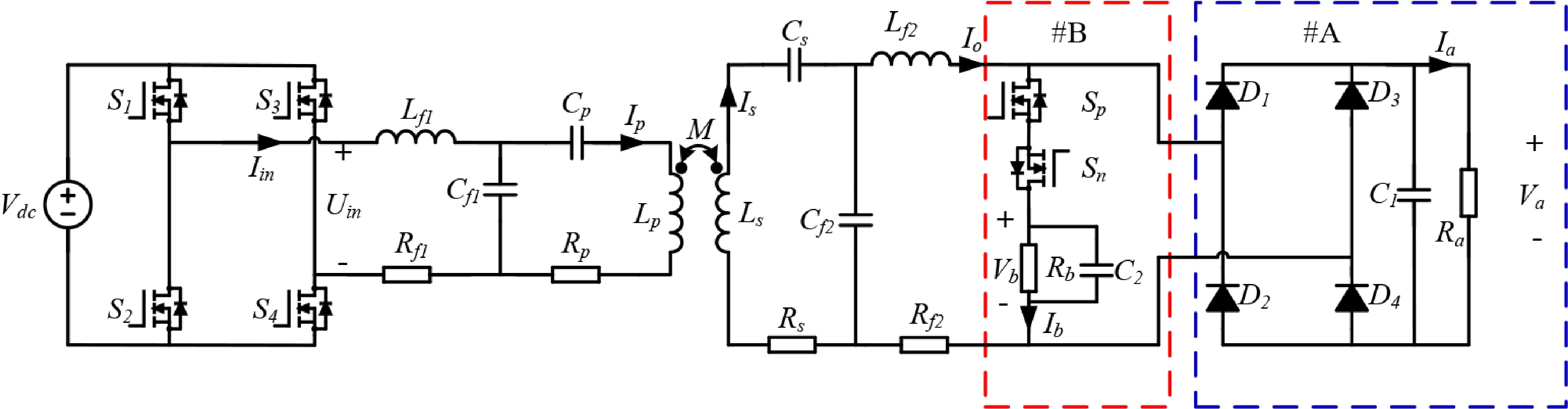
Figure 1.
Topology of the dual-load WPT system with constant-voltage and constant-current capabilities.
For the #A output circuit, the constant current output can be achieved by utilizing the characteristics of the LCC-LCC compensation topology. In the #B output circuit, the positive half-wave rectifier outputs a forward voltage by controlling switch SP, while the negative half-wave rectifier outputs a reverse voltage by controlling switch Sn.
Analysis of transmission performance in LCC-LCC dual-load WPT systems
-
Compared to conventional multi-load WPT systems operating in 'single-to-multiple' or 'multiple-to-multiple' power delivery modes, the circuit configuration in Fig. 2 eliminates multi-coil coupling by adopting a single-to-single power transfer architecture. Specifically, this topology employs only one transmitter and one receiver, thereby eliminating undesirable cross-coupling effects between multiple coils on output power regulation.
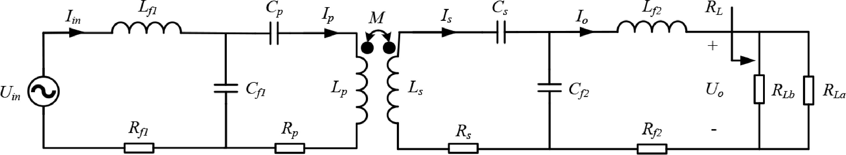
Figure 2.
Equivalent circuit model.
Here, Uin denotes the inverter output voltage. To simplify analysis, the theoretical derivation employs the fundamental harmonic approximation (FHA) method. By controlling the inverter through phase-shifted modulation (PSM), the fundamental component of the inverter output voltage can be expressed in phasor form as:
$ {U}_{in}=\dfrac{2\sqrt{2}{V}_{dc}}{\pi }\sin \dfrac{\delta }{2}\angle {0}^{\circ } $ (1) Where
$ \delta $ Applying Kirchhoff's Voltage Law (KVL) to the equivalent model shown in Fig. 2:
$ \left[\begin{array}{l} {U}_{in}\\ 0\\ 0\\ 0 \end{array}\right]=\left[\begin{matrix} {R}_{f1}+j\omega {L}_{f1}+\dfrac{1}{j\omega {C}_{f1}} & -\dfrac{1}{j\omega {C}_{f1}} & 0 & 0\\ -\dfrac{1}{j\omega {C}_{f1}} & {R}_{P}+j\omega {L}_{P}+\dfrac{1}{j\omega {C}_{P}}+\dfrac{1}{j\omega {C}_{f1}} & -j\omega M & 0\\ 0 & -j\omega M & {R}_{S}+j\omega {L}_{S}+\dfrac{1}{j\omega {C}_{S}}+\dfrac{1}{j\omega {C}_{f2}} & -\dfrac{1}{j\omega {C}_{f2}}\\ 0 & 0 & -\dfrac{1}{j\omega {C}_{f2}} & {R}_{L}+{R}_{f2}+j\omega {L}_{f2}+\dfrac{1}{j\omega {C}_{f2}} \end{matrix} \right]\cdot \left[\begin{array}{l} {I}_{in}\\ {I}_{P}\\ {I}_{S}\\ {I}_{o} \end{array}\right] $ (2) where, RL = RLa//RLb, RLa and RLb represent the equivalent input impedances of #A output circuit and #B output circuit, respectively, satisfying:
$ {R}_{La}=\dfrac{8}{{\pi }^{2}}{R}_{a},{R}_{Lb}=\dfrac{U_{0}^{2}}{V_{b}^{2}}{R}_{b} $ (3) where, Uo denotes the voltage across equivalent load RL, and Vb represents the output voltage of the half-wave rectifier circuit.
To maintain system resonance and reduce reactive power losses, both transmitter and receiver must operate at resonance, with the system angular frequency ωS matching the inverter operating frequency ω. The resonant components must satisfy:
$ \begin{cases} j\omega {L}_{f1}+\dfrac{1}{j\omega {C}_{f1}}=0\\ j\omega {L}_{P}+\dfrac{1}{j\omega {C}_{P}}+\dfrac{1}{j\omega {C}_{f1}}=0\\ j\omega {L}_{S}+\dfrac{1}{j\omega {C}_{S}}+\dfrac{1}{j\omega {C}_{f2}}=0\\ j\omega {L}_{f2}+\dfrac{1}{j\omega {C}_{f2}}=0 \end{cases} $ (4) Substituting Eq. (4) into Eq. (2) yields the expressions for the currents in each loop:
$ \begin{cases} {I}_{in}=\dfrac{{U}_{in}}{{Z}_{in}}\\ {I}_{p}=\dfrac{-j\omega {L}_{f1}({\omega }^{2}{L}_{f2}{}^{2}+{R}_{L}{R}_{S}+{R}_{S}{R}_{f2})}{{\omega }^{2}({L}_{f2}{}^{2}{R}_{P}+{M}^{2}{R}_{L}+{M}^{2}{R}_{f2})+{R}_{P}{R}_{S}({R}_{L}+{R}_{f2})}{I}_{in}\\ {I}_{S}=\dfrac{{\omega }^{2}M{L}_{f1}({R}_{L}+{R}_{f2})}{{\omega }^{2}({L}_{f2}{}^{2}{R}_{P}+{M}^{2}{R}_{L}+{M}^{2}{R}_{f2})+{R}_{P}{R}_{S}({R}_{L}+{R}_{f2})}{I}_{in}\\ {I}_{o}=\dfrac{j{\omega }^{3}M{L}_{f1}{L}_{f2}}{{\omega }^{2}({L}_{f2}{}^{2}{R}_{P}+{M}^{2}{R}_{L}+{M}^{2}{R}_{f2})+{R}_{P}{R}_{S}({R}_{L}+{R}_{f2})}{I}_{in} \end{cases} $ (5) According to Eq. (5), the equivalent input impedance of the dual-load WPT system can be obtained as:
$ {Z}_{in}={R}_{f1}+\dfrac{{\omega }^{2}{L}_{f1}{}^{2}{R}_{S}({R}_{L}+{R}_{f2})+{\omega }^{4}{L}_{f1}{}^{2}{L}_{f2}{}^{2}}{({R}_{P}{R}_{S}+{\omega }^{2}{M}^{2})({R}_{L}+{R}_{f2})+{\omega }^{2}{L}_{f2}{}^{2}{R}_{P}} $ (6) And the expression for the equivalent voltage Uo at the load side after passing through the compensation network can be derived as:
$ {U}_{o}=\dfrac{j{\omega }^{3}M{L}_{f1}{L}_{f2}{R}_{L}}{{\omega }^{2}({L}_{f2}{}^{2}{R}_{P}+{M}^{2}{R}_{L}+{M}^{2}{R}_{f2})+{R}_{P}{R}_{S}({R}_{L}+{R}_{f2})}{I}_{in} $ (7) According to Eq. (5), the expressions for the output power and transmission efficiency of the equivalent load RL can be derived as:
$ \begin{cases} {P}_{o}=\dfrac{e{\omega }^{2}{M}^{2}U_{in}^{2}{R}_{L}}{{[a{{R}_{f1}}+{{\omega }^{2}}(b{{R}_{f1}}+c{{R}_{f1}}+d)+e]}^{2}}\\ \eta =\dfrac{e{\omega }^{2}{M}^{2}{R}_{L}}{(a+{\omega }^{2}(b+c))(a{R}_{f1}+{\omega }^{2}(b{R}_{f1}+c{R}_{f1}+d)+e)} \end{cases} $ (8) where, parameters a–e are defined as:
$ \begin{cases} a={R}_{P}{R}_{S}({R}_{L}+{R}_{f2})\\ b={M}^{2}({R}_{L}+{R}_{f2})\\ c=L_{f2}^{2}{R}_{P}\\ d=L_{f1}^{2}{R}_{S}({R}_{L}+{R}_{f2})\\ e={\omega }^{4}L_{f1}^{2}L_{f2}^{2} \end{cases} $ (9) For #A output circuit, the voltage gain of the full-bridge rectifier is given by:
$ {I}_{a}=\dfrac{{V}_{a}}{{R}_{a}}=\dfrac{\sqrt{2}\pi {U}_{o}}{4{R}_{a}} $ (10) Analysis of half-wave rectifier circuit
-
Compared to the #A output circuit, the #B output circuit employs two anti-series power switches (SP and Sn) forming a half-wave rectifier. This topology enables bidirectional voltage regulation to meet load polarity requirements. Figure 3 illustrates the operational modes of Output #B.
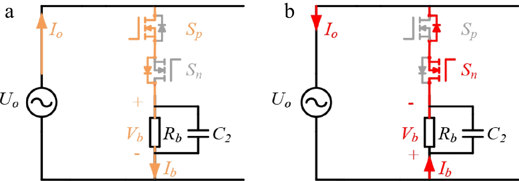
Figure 3.
Equivalent circuit of #B output circuit. (a) Forward conduction mode. (b) Reverse conduction mode.
Mode 1: Forward conduction mode
In this mode, the positive half-wave rectifier operates. The power switch Sn is turned off, and the body diode anti-parallel to switches Sp and Sn forms a forward conduction path. The output current Ib of the #B output circuit is positive, providing a forward output voltage for the load. This is shown in Fig. 3a.
Mode 2: Reverse conduction mode
In this mode, the negative half-wave rectifier operates. Switch Sp is turned off, and the body diodes anti-parallel to Sn and Sp form a reverse conduction path. The output current Ib of the #B output circuit is negative, enabling it to provide a reverse output voltage for the load. The schematic diagram is shown in Fig. 3b.
As can be seen from Fig. 3, since two half-wave rectifiers are integrated into one channel, the polarity switching of the load output voltage can be achieved simply by controlling the turn-on and turn-off of two anti-parallel power switching devices. Meanwhile, the designed response control method is more concise, which will be explained in the next section.
The output voltage of the positive half-wave rectifier in #B output circuit is given by:
$ V_b = \dfrac{1}{2\pi} \int_{0}^{2\pi D_{sp}} \sqrt{2} U_o \sin(\omega t) d\omega t = \dfrac{\sqrt{2} U_o}{2\pi} \left(1 - \cos\left(2\pi D_{sp}\right)\right) $ (11) where, Dsp is the duty cycle of switch SP's drive signal during the positive half-cycle. Similarly, the output voltage of the negative half-wave rectifier in #B output circuit is expressed as:
$ -V_b = -\dfrac{1}{2\pi} \int_{\pi}^{\pi + 2\pi D_{sp}} \sqrt{2} U_o \sin(\omega t) d\omega t= \dfrac{\sqrt{2} U_o}{2\pi} \left(1 - \cos\left(2\pi D_{sp}\right)\right) $ (12) From the above analysis, it can be concluded that the #A output circuit can maintain a constant current Ia by virtue of the characteristics of the LCC-LCC compensation network. For the output #B, a stable output voltage Vb can be achieved by determining the switching frequency and duty cycle of the control switches Sp and Sn.
Composite constant voltage and current output control strategy
-
As derived from Eqs (10), (11), and (12), the output current Ia of the output #A and the output voltage Vb of the #B output circuit can be regulated independently.
By substituting Eqs (1), (5), and (10) into Eq. (15) while neglecting the coil resistance, the inverter output voltage, equivalent load RLa of the output #A, ac-side current Io, and full-wave rectifier output current Ia in the dual-load WPT system can be reformulated as:
$ \begin{cases} {U}_{in}=\dfrac{2\sqrt{2}}{\pi }{V}_{dc}\sin \dfrac{\delta }{2}\\ {I}_{o}=\left| \dfrac{M{U}_{in}}{\omega {L}_{f1}{L}_{f1}}\right| \\ {I}_{a}=\dfrac{\sqrt{2}\pi {I}_{o}{R}_{La}}{4{R}_{a}} \end{cases} $ (13) The expression for the inverter phase-shift angle δ can be derived as:
$ \delta =2\arcsin \left(\dfrac{{\pi }^{2}\omega {L}_{f1}{L}_{f2}{I}_{a}}{8M{V}_{dc}}\right) $ (14) To achieve constant-current output for #A output circuit and constant-voltage output for #B output circuit with independent power control, it is essential to enhance the system's disturbance rejection capability. Therefore, selecting an appropriate control strategy is crucial. This section focuses on improving the constant current control performance of #A output circuit by combining feedforward PI control with phase-shift modulation, while #B output circuit employs conventional PI control for constant-voltage regulation.
Design of feedforward PI controller
-
In the dual-load WPT system, the presence of delays and errors in PI control can reduce the system's control tracking performance. To address this issue, a feedforward controller is introduced to improve the system's response speed and control accuracy. Its core idea is to reduce output deviations by predicting and compensating for changes in external disturbances or system inputs in advance. PI control can compensate for system errors and disturbances, while feedforward control can predict the system's output in advance and perform compensation simultaneously. Through the combined action of PI control and the feedforward link, high-precision constant current output control of the dual-load WPT system can be achieved.
Figure 4 illustrates the control schematic combining PI control with feedforward compensation. In this diagram, R(s) and Y(S) represent the input and output variables, respectively, Gf (S) denotes the transfer function of the feedforward controller, Kp + Ki/S corresponds to the transfer function of the PI controller, and Gp (S) describes the transfer function of the controlled plant. The error signal E(S) is defined as E(S) = R(S) − Y(S).
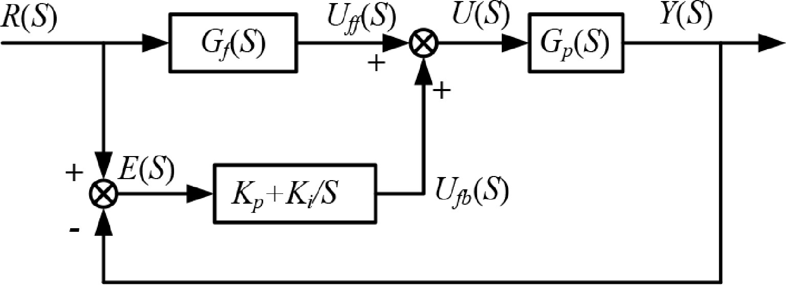
Figure 4.
Schematic diagram of feedforward PI control.
From Fig. 4, the transfer function of the feedforward control can be derived as:
$ {U}_{ff}(S)={G}_{f}(S)R(S) $ (15) Similarly, the transfer function of the PI control can be obtained as:
$ {U}_{fb}(S)=\left({K}_{p}+\dfrac{{K}_{i}}{S}\right)E(S) $ (16) By superimposing the feedforward and PI control loop equations shown in Eqs (15) and (16), the total control output can be expressed as:
$ U(S)={U}_{ff}(S)+{U}_{fb}(S) $ (17) Based on the aforementioned theoretical analysis, the closed-loop output expression can be derived as:
$ Y(S)=\dfrac{{G}_{p}(S)\left[{G}_{f}(S)+\left({K}_{p}+\dfrac{{K}_{i}}{S}\right)\right]R(S)}{1+{G}_{p}(S)\left({K}_{p}+\dfrac{{K}_{i}}{S}\right)} $ (18) In Eq. (18), the feedforward path Gf(S) enables direct generation of control actions from the reference input R(S), achieving rapid command tracking through immediate response to input variations. Simultaneously, the error signal E(S) facilitates adaptive control adjustment to suppress disturbances and eliminate steady-state errors. The synergistic integration of feedforward and PI control enhances the system's dynamic response speed while ensuring robust performance and improved disturbance rejection capability.
For #B output circuit, constant-voltage output can be achieved by implementing real-time detection of the voltage Uo across the receiver equivalent load RL, followed by PI control regulation according to Eqs (11) and (12).
The overall control block diagram proposed in this paper is shown in Fig. 5.
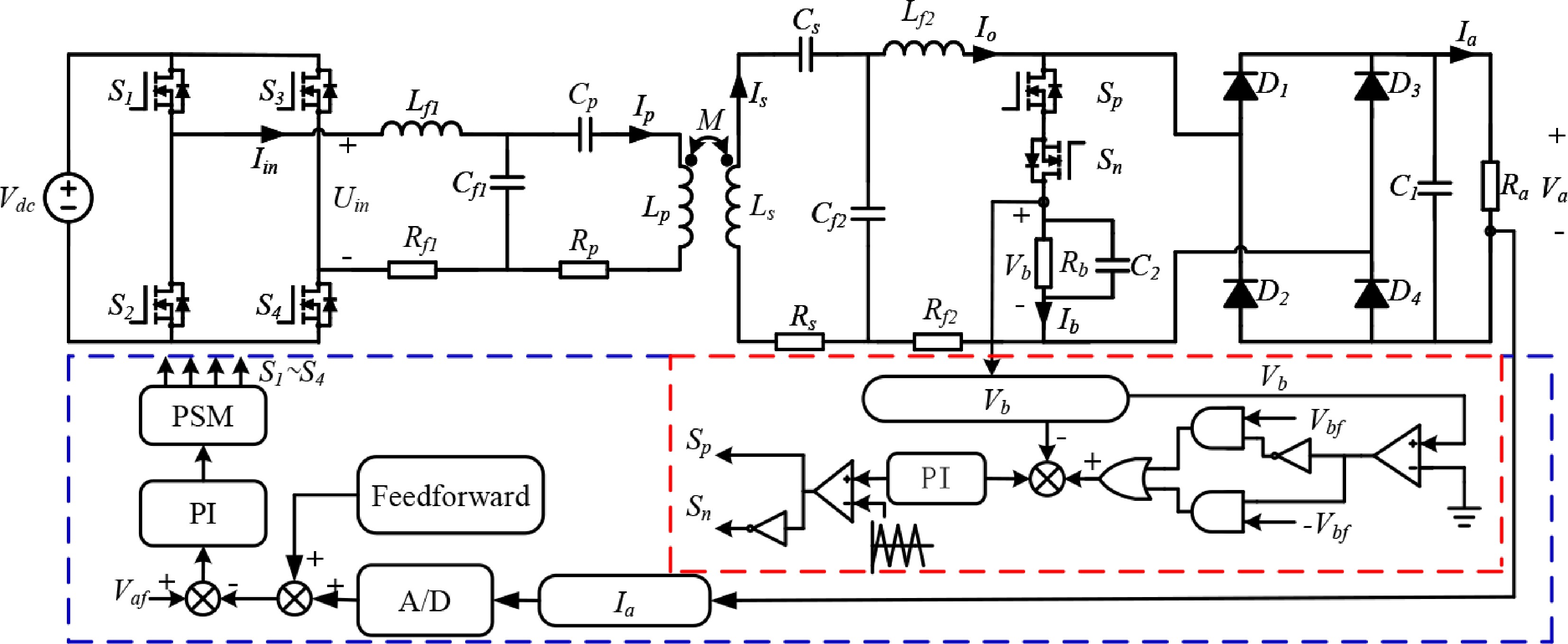
Figure 5.
Schematic diagram of the composite control strategy for dual-load WPT systems.
In Fig. 5, for #A output circuit, the measured output current Ia is acquired through the current sensing circuit and the A/D conversion module. This signal is then processed by the feedforward compensation block before being compared with the reference current Iaf. The resulting error signal is fed into the PI controller, whose output is transmitted to the phase-shift modulation module for conduction angle calculation. This modulated signal ultimately drives the full-bridge inverter circuit to regulate Io, thereby controlling the output current Ia.
For #B output circuit, the load voltage Vb across Rb is measured and compared with the reference voltage Vbf (or −Vbf). The resulting error signal is processed by the PI controller, which regulates the switching operations of Dsp and Dsn to adjust Vb. This control methodology enables independent multi-channel power output while maintaining excellent system stability.
Based on the above analysis, the design flowchart of system parameters is illustrated in Fig. 6.
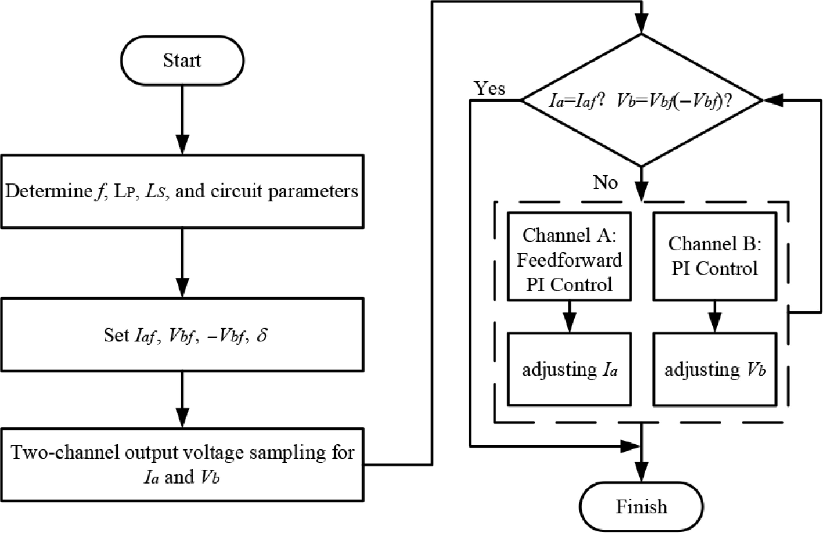
Figure 6.
System operation flowchart.
-
To validate the feasibility of the proposed composite constant-voltage and current control method for the dual-load WPT system, an experimental prototype was constructed as shown in Fig. 7.
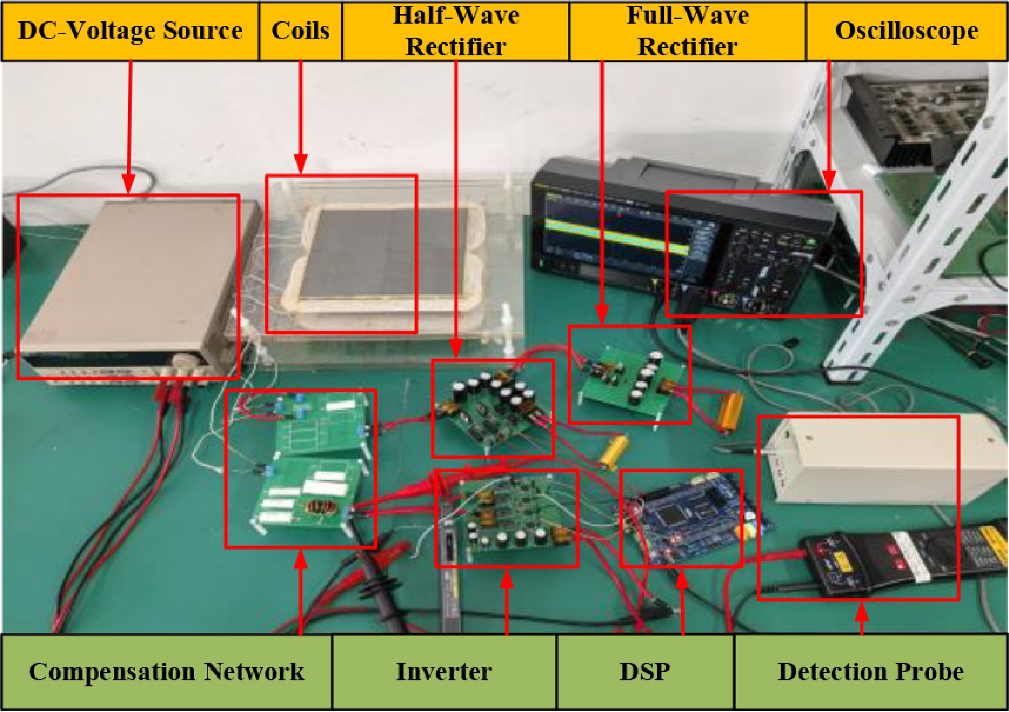
Figure 7.
Experimental platform.
The entire system consists of a high-frequency inverter, an LCC-LCC compensation circuit, transmitting and receiving coils, a half-wave rectifier, a full-bridge rectifier, loads, and a control circuit, with the system resonance frequency set to 85 KHz. To ensure the generation of high-frequency power, gallium nitride (GaN) power switching devices with high switching frequency and low switching loss are used to form the high-frequency inverter circuit and the half-wave rectifier circuit. The control algorithm is implemented using the TMS320F28335 DSP from TI. Table 1 presents the specific experimental parameters of the system.
Table 1. Experimental parameters.
Item Value Item Value Vdc 30 V f 85 KHz LP 247.40 μH CP 16.16 nF LS 110.69 μH CS 45.13 nF Lf1 30 μH Cf1 116.86 nF Lf2 33 μH Cf2 106.24 nF RP 0.2 Ω Rf1 0.07 Ω RS 0.14 Ω Rf2 0.09 Ω ZVS verification
-
The composite CV/CC control method proposed in this paper is implemented by phase-shift voltage regulation using the inverter at the transmitter. Through the built experimental platform, under the condition that Ra = Rb = 10 Ω and with different reference output currents Ia and output voltages Vb, the waveforms of the inverter output voltage Uin and output current Iin at the transmitter are shown in Fig. 8. As can be seen, when the system output reference value changes, tracking of the output reference value can be achieved by adjusting the phase-shift angle of the inverter, and the system can realize Zero Voltage Switching (ZVS).
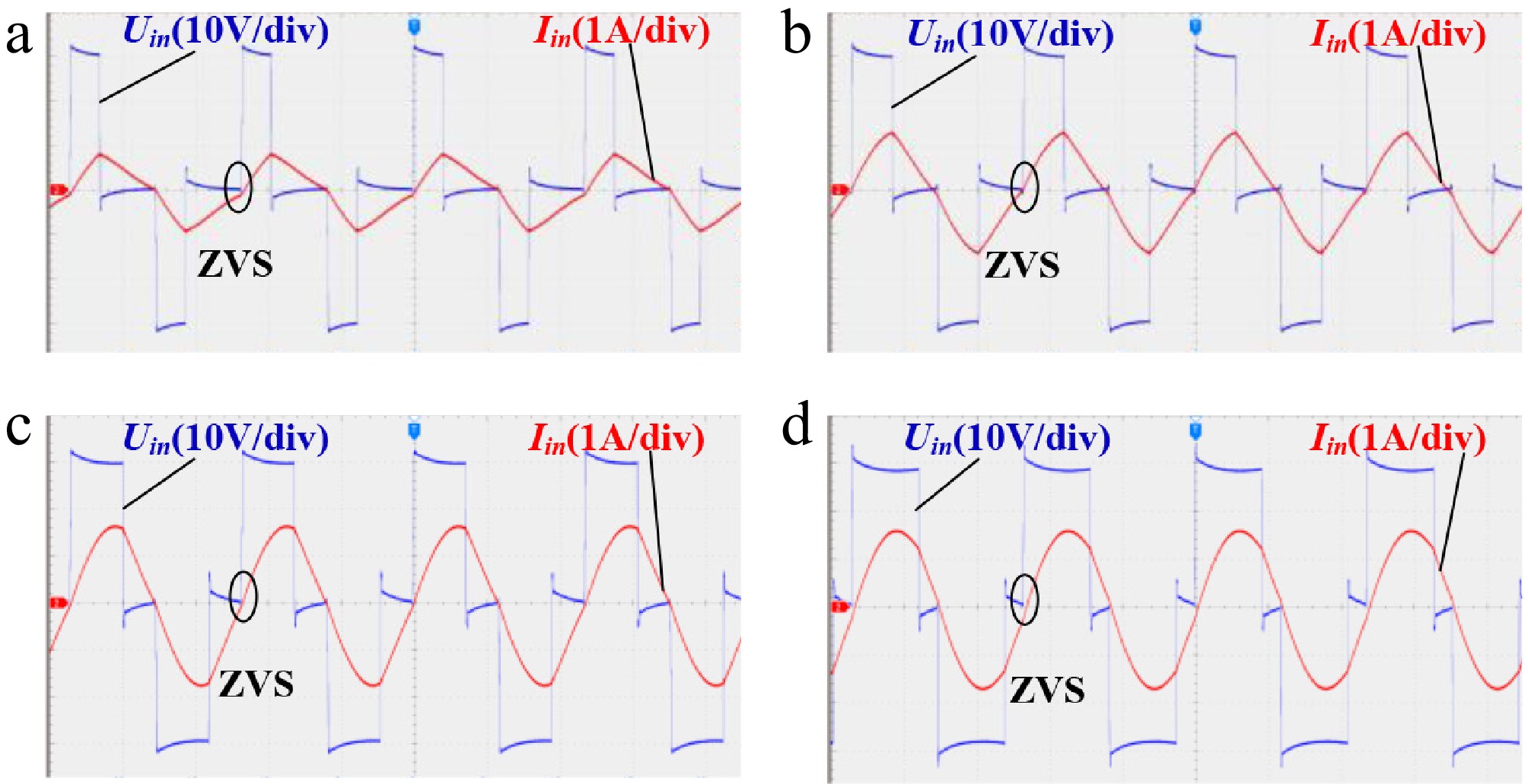
Figure 8.
Waveforms of the inverter's output voltage and current under different reference values. (a) Ia = 1 A,Vb = ±5 V. (b) Ia = 1.2 A,Vb = ±10 V. (c) Ia = 2 A,Vb = ±15 V. (d) Ia = 2.4 A,Vb = ±25 V.
Analysis on the control effect of composite constant voltage and current
-
This paper proposes a composite CV/CC control method that can maintain the output current Ia of Circuit #A and the output voltage Vb of Circuit #B constant. Notably, for Vb, positive and negative polarity switching can be performed according to load requirements. Therefore, studying the effect of composite CV/CC control is of great necessity, which can be specifically divided into two parts: first, verifying whether Ia and Vb can be independently controlled, that is, whether the output power of Circuits #A and #B can realize independent power regulation; second, verifying whether the amplitude of Vb remains consistent after polarity switching, that is, the magnitude of the output power remains unchanged before and after polarity switching, and only the power direction changes.
Figure 9 shows the waveforms when the reference value of the output current Ia remains unchanged while the reference value of the output voltage Vb changes. As can be seen from the figure, Ia always remains at the set reference value, and at the same time, Vb can also track different reference output voltages.
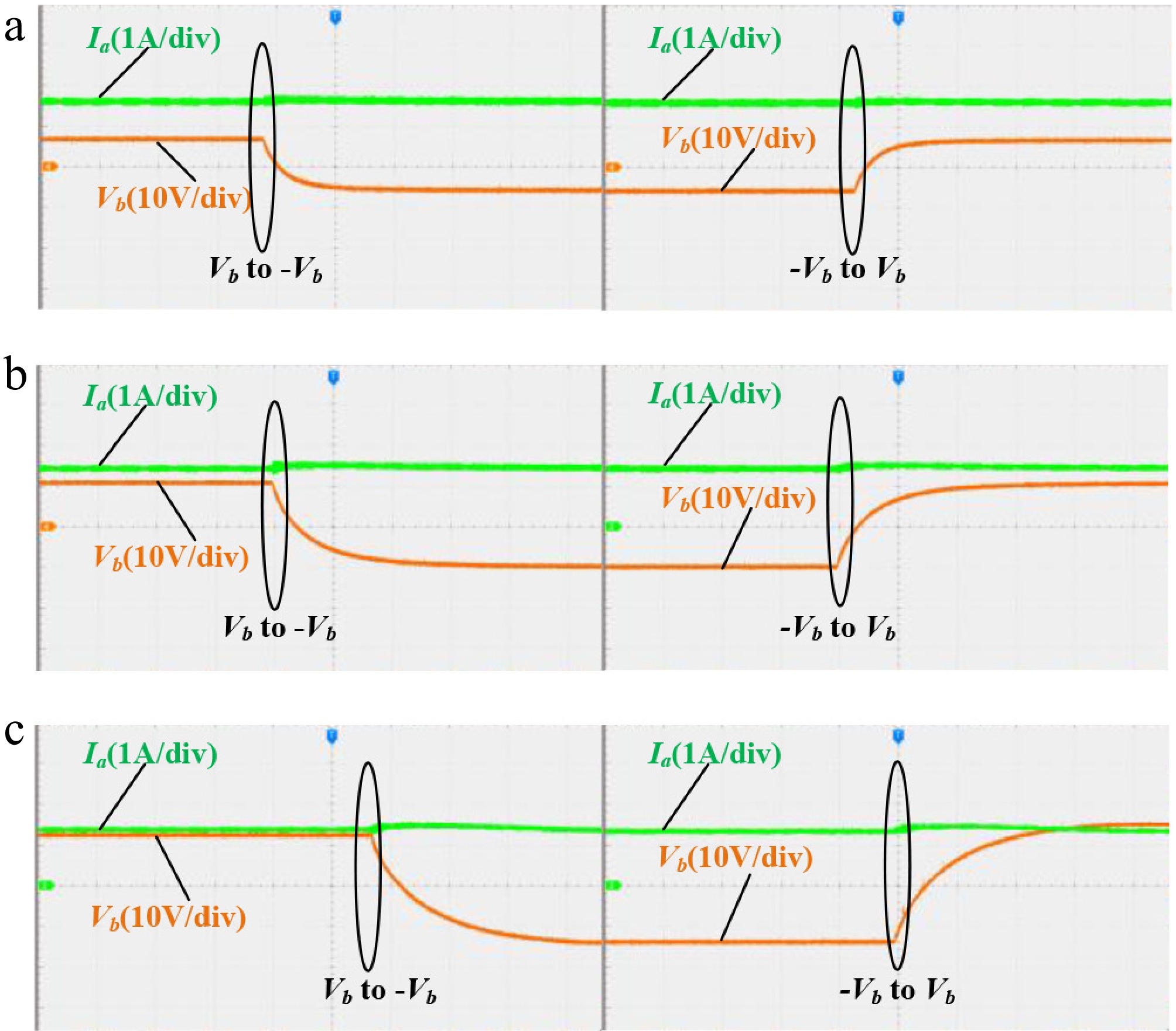
Figure 9.
Verification waveforms of independent power regulation. (a) Ia = 1.6 A,Vb = ±7.5 V. (b) Ia = 1.6 A, Vb = ±10 V. (c) Ia = 1.6 A,Vb = ±15 V.
Fixing the output voltage of Vb at ±15 V, the experimental waveforms when the reference value of Ia's output is changed are shown in Fig. 10. It can be seen that no matter how the reference current of Ia changes, it does not affect the output of Vb, which verifies that the output power of Circuits #A and #B can achieve independent control, with almost no mutual influence between them.
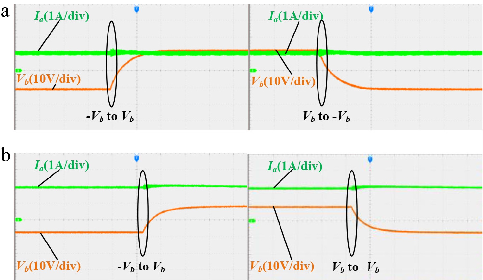
Figure 10.
Experimental waveforms of Vb polarity switching. (a) Ia = 1.2 A,Vb = ±10 V. (b) Ia = 2 A,Vb = ±10 V.
By combining the experimental waveforms of Ia and Vb shown in Figs 9 and 10, the effect of the composite CV/CC control method can be verified. Furthermore, through a comprehensive comparison of the experimental waveforms in the two figures, it can be seen that for Vb, whether it is switching from positive polarity voltage to negative polarity voltage or from negative polarity voltage to positive polarity voltage, its amplitude remains consistent before and after polarity switching. This further proves that the system's output power is not affected by polarity switching.
The measured system transmission efficiency before and after the polarity switching points is shown in Fig. 11. As can be seen, when Ra and Rb vary within a certain range, the system transmission efficiency remains at a high level overall, which indirectly indicates that the system transmission efficiency is not affected by the polarity switching of Vb.
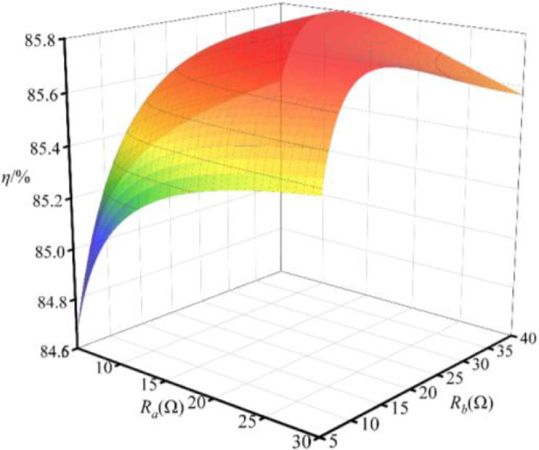
Figure 11.
System transmission efficiency.
Dynamic performance
-
To study the dynamic performance of the system, with the output reference values at Ra = Rb = 10 Ω (Ia = 1.6 A and Vb = ±10 V) still used as the reference, Fig. 12 shows the dynamic response diagrams when Ra and Rb change, respectively. Figure 12a−c indicate that when Ra changes from 10 Ω→5 Ω→10 Ω, 10 Ω→20 Ω→10 Ω, and 20 Ω→10 Ω→20 Ω, both Ia and Vb can reach the set reference values. The system only has slight fluctuations when the load changes, and polarity switching of Vb at different times does not impact the amplitude of Vb. Figure 12d–f demonstrate that when Rb changes from 10 Ω→5 Ω→10 Ω, 10 Ω→20 Ω→10 Ω, and 20 Ω→10 Ω→20 Ω, the composite CV/CC control method can maintain Ia and Vb constant. The system has no obvious overshoot and can adapt to load variation scenarios.
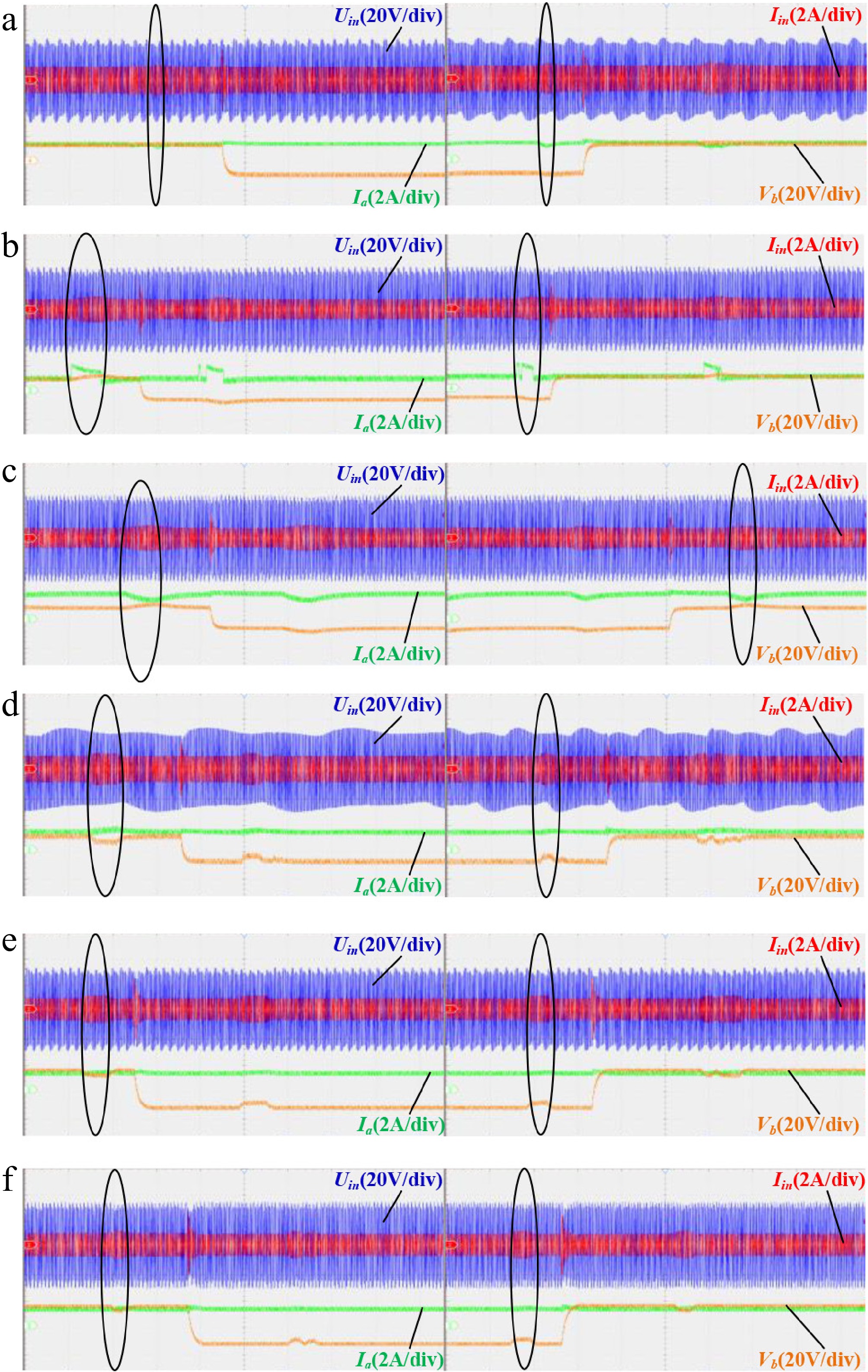
Figure 12.
Dynamic response of the system. (a) Ra: 10 Ω→5 Ω→10 Ω. (b) Ra: 10 Ω→20 Ω→10 Ω. (c) Ra: 20 Ω→10 Ω→20 Ω. (d) Rb: 10 Ω→5 Ω→10 Ω. (e) Rb: 10 Ω→20 Ω→10 Ω. (f) Rb: 20 Ω→10 Ω→20 Ω.
-
The composite CV/CC control method proposed in this paper can provide dual-load WPT systems with stable output voltage and output current. The two output controllers operate in a decoupled manner, and their output powers can be independently adjusted. Notably, a novel half-wave rectifier is designed, which can supply power to loads requiring voltage polarity switching and features convenience and cost-effectiveness. This work provides a new approach to addressing relevant issues in multi-load WPT systems.
-
To address the challenges of cross-coupling interference between coils and independent power regulation in conventional multi-load WPT systems, this paper proposes an innovative half-wave rectifier capable of output voltage polarity reversal and develops a composite constant-voltage and current control method for dual-output independent power regulation. The proposed solution offers a novel approach to resolving power control limitations in multi-load WPT systems, with the following key advancements:
(1) Proposes a novel active half-wave rectifier that achieves programmable output voltage polarity switching by controlling the switching states of two anti-series power semiconductor devices. The operational principles and control methodology for this rectifier topology are comprehensively established.
(2) A composite constant-voltage and current output control method is proposed. Feedforward PI control is adopted for phase-shift voltage regulation to adjust the inverter output voltage, thereby controlling a constant-current output. With the equivalent load voltage at the receiving end as the carrier, another constant-voltage output is realized through PI control.
It is worth mentioning that the composite CV/CC control method proposed in this paper still requires two controllers. Future research can further consider optimizing the control scheme, where regulation of output voltage and current can be achieved by only applying a controller at the transmitter.
This research was partially supported by the General Project of Chongqing Natural Science Foundation (Grant No. CSTB2024NSCQ-MSX0382), the Science and Technology Research Project of Chongqing Municipal Education Commission (Grant No. KJQN202201103), and the Joint-funded Project of Chongqing University of Technology (Grant Nos gzlcx20253187, gzlcx20243105).
-
The authors confirm their contributions to the paper as follows: study conception and design: Dong Y; data collection: Wang H, Zhang L, Ma S; analysis and interpretation of results: Peng Z, Cai Y, Hu J; draft manuscript preparation: Wang H, Dong Y. All authors reviewed the results and approved the final version of the manuscript.
-
The datasets generated during the current study are available from the corresponding author upon reasonable request.
-
The authors declare that they have no conflict of interest.
- Copyright: © 2026 by the author(s). Published by Maximum Academic Press, Fayetteville, GA. This article is an open access article distributed under Creative Commons Attribution License (CC BY 4.0), visit https://creativecommons.org/licenses/by/4.0/.
-
About this article
Cite this article
Wang H, Dong Y, Peng Z, Cai Y, Ma S, et al. 2026. Research on constant voltage and constant current dual-load wireless power transfer system based on composite control method. Wireless Power Transfer 13: e011 doi: 10.48130/wpt-0026-0001 

Research on constant voltage and constant current dual-load wireless power transfer system based on composite control method
- Received: 11 September 2025
- Revised: 30 October 2025
- Accepted: 29 December 2025
- Published online: 29 April 2026
Abstract: Existing wireless power transfer (WPT) systems often fail to simultaneously achieve constant-voltage (CV) and constant-current (CC) outputs when charging multiple devices. To address this limitation, this paper proposes a dual-load WPT system with CV and CC characteristics. The system comprises a full-bridge rectifier circuit for CC output and a novel half-wave rectifier circuit for CV output, along with a composite CV/CC control method to independently regulate power across the two output circuits. First, the power transfer characteristics of the proposed circuit topology are analyzed, and the operational principles of the novel half-wave rectifier are elucidated. Second, a transfer function model of the dual-load WPT system is established, and the composite CV/CC control strategy is introduced: feedforward PI control with phase-shift voltage regulation enables CC output for the full-bridge rectifier circuit, while PI control ensures CV output for the half-wave rectifier circuit. Finally, an experimental prototype is constructed to validate the power transfer characteristics and the composite CV/CC control method. Experimental results demonstrate the feasibility and stability of the proposed approach.
-
Key words:
- Wireless power transfer /
- Dual-load /
- Half-wave rectifier /
- Constant voltage and current