


-
The rapid densification of urban infrastructure, particularly in utility tunnels and rail transit networks, has underscored the critical need for robust operation and maintenance (O&M) protocols. However, these environments are frequently characterized by hostile conditions—ranging from toxic gas accumulation to water ingress—and involve dispersed equipment clusters that complicate management[1]. Consequently, reliance on manual inspection is increasingly untenable becausof of the prohibitive labor costs, inefficiency, and, most critically, the severe occupational hazards posed to personnel. To mitigate these issues, autonomous robotic inspection systems have been widely adopted as the primary solution for routine maintenance[2], effectively isolating human operators from dangerous environments while enhancing monitoring precision.
Despite their operational benefits, the power supply for these robots remains a bottleneck. Conventional conductive charging and battery swapping methods are hampered by their inherent limitations. Specifically, the requisite physical coupling in wired systems makes them vulnerable to connector degradation, mechanical wear, and electric arcing, especially in the presence of environmental contaminants like dust and moisture. Furthermore, the maintenance of such contact-based interfaces is labor-intensive and prone to failure through cable entanglement or oxidation[3−7]. To overcome these physical constraints, wireless power transfer (WPT) has emerged as a superior alternative. By eliminating galvanic connections, WPT technology intrinsically avoids the risks of generating sparks and contact wear. Its encapsulated nature ensures immunity to humidity and corrosive gases, thereby significantly extending system longevity and reliability. Moreover, the absence of tethered cables grants robots unrestricted mobility, making WPT an ideal, maintenance-free energy solution for complex inspection scenarios.
To guarantee the operational sustainability of inspection robots, the charging interface must adhere to a strict battery management protocol, primarily to balance charging velocity with electrochemical safety. The standard constant current–constant voltage (CC-CV) hybrid profile is universally implemented to mitigate thermal runaway risks during the initial depletion phase, when internal impedance is minimal, and to avert electrolyte degradation or overpotential hazards near full capacity[8]. By regulating the charging trajectory from a current-limiting stage to a voltage-clamping phase, this strategy optimizes energy throughput while preserving the battery's cycle life against the rigorous duty cycles of robotic applications[9−11]. In the pursuit of implementing this ideal charging characteristic within WPT frameworks, the existing methodologies can be systematically classified into several categories.
To address the limitations of conventional charging approaches, the first category of control methods employs real-time closed-loop mechanisms, including a variable capacitor is connected in series on the secondary side[12,13], frequency control[14−15] phase-shift control[16], and pulse density modulation (PDM)[17]. Although these techniques can achieve CV or CC output, they generally require wireless communication to acquire the battery status in real time for feedback control, which considerably restricts their applicability in practice. Moreover, the incorporation of control strategies increases the system's complexity and may adversely affect overall reliability. The second category of methods leverages the inherent characteristics of circuit topologies to achieve load-independent automatic CV–CC switching without relying on control algorithms. For instance, an additional clamping coil on the transmitter side of an series–series (S–S) (resonant converter / compensation network) topology is proposed[18], eliminating the need for communication and control circuits between the primary and secondary sides. However, the coupling issues among multiple coils remain inadequately addressed. A reconfigurable hybrid wireless charging system is proposed[19], which achieves CV or CC output by altering the topological configuration: The system can be configured as an inductor–capacitor–capacitor (LCC) (resonant tank topology) –S and S–LCC hybrid for CV output, or switched to S–S and LCC–LCC hybrid for CC output. Nevertheless, this approach still partially relies on communication and control strategies.
To address the aforementioned technical limitations, this paper proposes a multi-stage wireless charging system with inherent CV and CC switching capability. The core contributions and advantages of the proposed system are summarized below.
This paper proposes a reconfigurable LCC-S-S topology, incorporating an intermediate coupler and a switch, to synthesize the specific output characteristics required for battery charging. The system is engineered to inherently provide CC and CV outputs, automatically adapting to the battery's load profile without external intervention. A distinctive feature of this design is that the mode transition is strictly governed by the intrinsic properties of the hardware topology rather than complex control algorithms. Consequently, this approach obviates the need for voltage/current feedback loops or wireless communication modules, thereby significantly reducing system complexity and cost while enhancing reliability through a decoupled magnetic structure.
-
To achieve automatic CV and CC switching in a WPT system, this paper proposes a magnetically coupled mechanism capable of reconfiguring between LCC-S-S and LCC-S topologies. The specific structure of the proposed coupler is illustrated in Fig. 1a. The transmitter coil (Lp), relay coil (L0), and receiver coil (Ls) are all designed as Q-type coils to improve the magnetic field's uniformity and coupling stability. Ferrite cores are placed on both the transmitter and receiver sides to enhance the magnetic coupling strength through their low-reluctance characteristics while effectively constraining stray magnetic fields. Furthermore, an aluminum shield is installed on the inspection robot's side to suppress electromagnetic leakage, thereby improving electromagnetic compatibility (EMC) and operational safety.
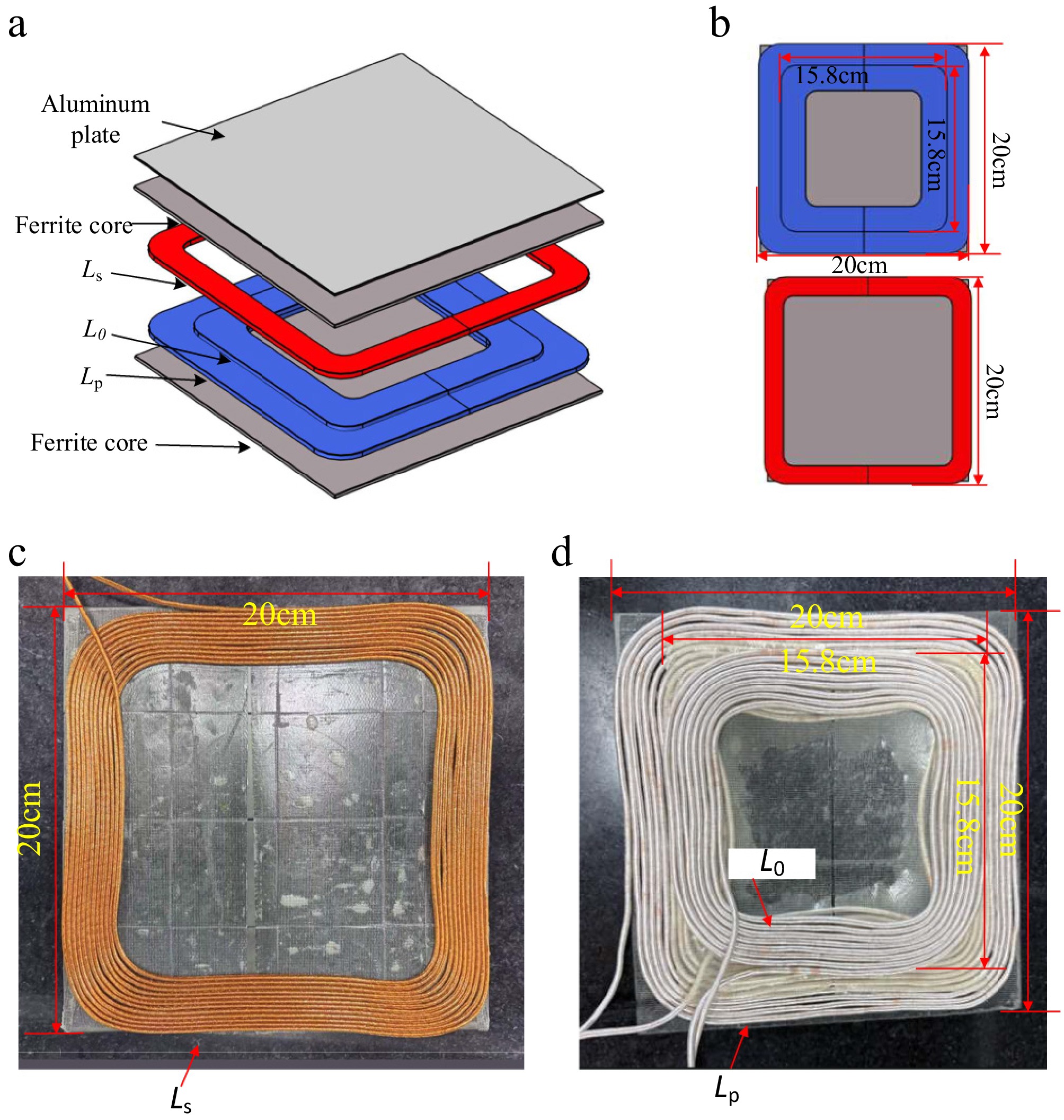
Figure 1.
The magnetic coupling structure: (a) Overview, (b) specific details, (c) picture of Ls, and (d) picture of Lp and L0.
For fabrication of the magnetic couplers, Litz wire was selected to minimize the skin effect. Specifically, the transmitting coil (Lp) and the intermediate coil (L0) were constructed using 450-strand Litz wire with an external diameter of 3 mm. In contrast, the secondary coil (Ls) used a slightly thinner 350-strand variant (2.5 mm in diameter). The geometric specifications and physical configurations are shown in Fig. 1b−d. Notably, as depicted in Fig. 1d, the intermediate coil is coaxially stacked directly atop the transmitting coil to ensure tight coupling. The optimized turn counts for the respective windings—denoted as Np, N0, and Ns—are fixed at 15, 8, and 12 turns, respectively, the detailed design derivation of which is described in a subsequent section.
-
To accommodate the stringent charging profiles of inspection robots' batteries, the WPT interface must dynamically transition between CC and CV modes. Conventional static compensation networks are inherently monolithic, typically supporting only a single output characteristic, which necessitates complex auxiliary control loops for multi-stage charging. To overcome this limitation, this paper proposes a reconfigurable hybrid architecture that synthesizes the LCC-S and LCC-S-S topologies. By leveraging a secondary-side rectification scheme, the system achieves autonomous state regulation in response to load fluctuations, ensuring a smooth transient response between CC and CV modes while preserving full-range zero voltage switching (ZVS).
The operational modality is governed by the state of the auxiliary switch S. The deactivation of S (open state) configures the network into the LCC-S topology, where the output voltage exhibits load-independent characteristics, thereby realizing the CV phase. Conversely, activating S (closed state) transforms the circuit into the LCC-S-S structure, yielding a load-independent output current that is essential for the CC phase. For analytical clarity, ideal component characteristics are assumed, disregarding ohmic losses in the inductive elements. Consequently, the charging trajectory is executed as follows: The process initiates with the LCC-S-S configuration for rapid CC replenishment and, upon reaching the voltage threshold, seamlessly transitions to the LCC-S configuration for CV maintenance. This dual-mode mechanism significantly optimizes both energy efficiency and the system's adaptability under varying load conditions.
Figure 2 illustrates the hybrid configuration of the proposed multi-stage topology, which enables reconfiguration between the LCC-S and LCC-S-S modes with a single switch. In this schematic, Lp, L0, and Ls represent the self-inductances of the transmitter coil, intermediate coil, and receiver coil, respectively. The LCC-S compensation topology (Compensation Path 1) is formed by Lp and Ls together with the compensation capacitors C1, Cp, and Cs, whereas the LCC-S-S topology (Compensation Path 2) consists of Lp, L0, and Ls with the compensation capacitors C1, Cp, and Cs. The mutual inductances are defined as MLp_Ls (between the transmitter and receiver coils), MLp_L0 (between the transmitter and intermediate coils), and ML0_Ls (between the intermediate and receiver coils). The switching S mechanism uses a bidirectional configuration comprising two anti-series metal–oxide–semiconductor field-effect Transistors (MOSFETs) (S1 and S2).
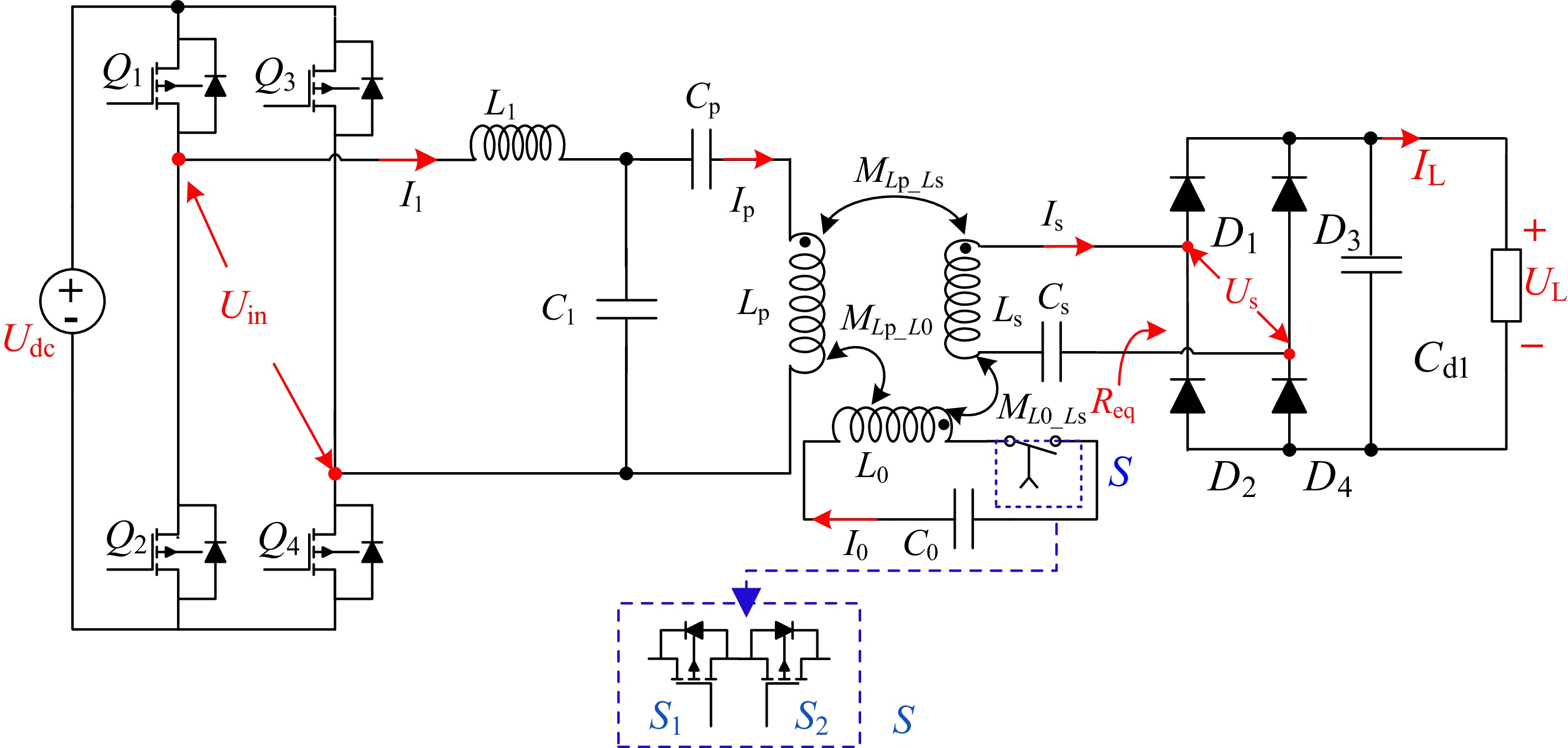
Figure 2.
Circuit diagram of the proposed WPT system.
By applying the fundamental harmonic approximation (FHA), the mathematical expressions for the inverter's output voltage (Uin), as well as the input voltage (Us) and current (Is) of the rectifier, are derived as follows:
$ {U}_{\text{in}}=\dfrac{2\sqrt{2}}{\pi }{U}_{\text{dc}}\sin \dfrac{\alpha }{2} $ (1) $ {U}_{\text{s}}=\dfrac{2\sqrt{2}}{\pi \omega }{U}_{\text{L}} $ (2) $ {I}_{\text{s}}=\dfrac{\sqrt{2}\pi }{4}{I}_{\text{L}} $ (3) $ {I}_{\text{p}}=\dfrac{2\sqrt{2}{U}_{\text{dc}}}{\pi {L}_{1}} $ (4) The system achieves automatic CV and CC output switching via the inherent characteristics of its compensation topology. Compensation Path 1 uses an LCC-S structure, which provides stable CV output because of its load-independent voltage characteristics. Compensation Path 2 adopts an LCC-S-S configuration, exhibiting ideal CC output, as its current remains largely unaffected by load variations. The system autonomously adjusts the dominant output path in response to changes in the load's impedance. As a result, a seamless transition between CC and CV modes is realized without requiring any external control circuits or auxiliary strategies. The corresponding equivalent circuit diagram is illustrated in Fig. 2.
The parameters of the two compensation paths are designed identically. Specifically, Lp resonates completely with C1, whereas Lp, C1, and Cp together form a complete resonant network. On the secondary side, Ls is in full resonance with Cs; similarly, the intermediate coil L0 resonates completely with C0:
$ \left\{\begin{aligned} & j\omega {L}_{1}+\dfrac{1}{j\omega {C}_{1}}=0\\ &j\omega {L}_{\text{p}}+\dfrac{1}{j\omega {C}_{1}}+\dfrac{1}{j\omega {C}_{\text{p}}}=0\\ &j\omega {L}_{\text{s}}+\dfrac{1}{j\omega {C}_{\text{s}}}=0\\ &j\omega {L}_{\text{0}}+\dfrac{1}{j\omega {C}_{\text{0}}}=0 \end{aligned}\right. $ (5) When the system is in CV mode and the switch S is disconnected, its compensation branch adopts an LCC-S structure. The equivalent circuit diagram is shown in Fig. 3.
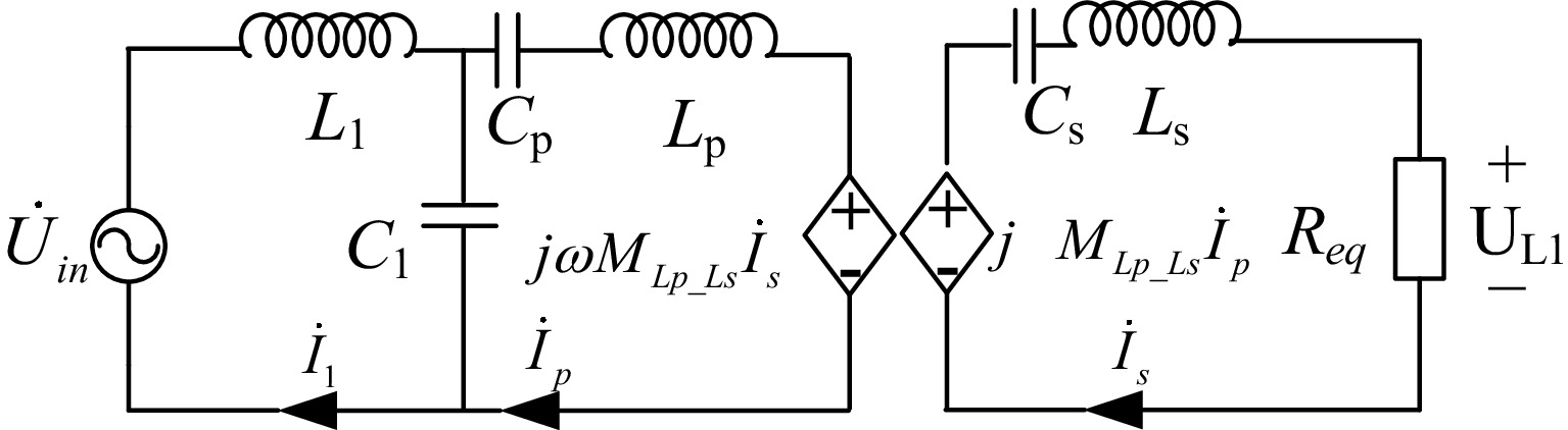
Figure 3.
Equivalent circuit with the LCC-S topology.
By applying Kirchhoff's voltage laws (KVL) in conjunction with the voltage transformation characteristics of the rectifier bridge, the governing circuit equations are formulated as follows:
$ \left\{\begin{aligned} &{U}_{\text{in}}={I}_{1}\left(j\omega {L}_{1}+\dfrac{1}{j\omega {C}_{1}}\right)-{I}_{\text{p}}\dfrac{1}{j\omega {C}_{1}}\\ &0={I}_{\text{p}}\left(j\omega {L}_{\text{p}}+\dfrac{1}{j\omega {C}_{1}}+\dfrac{1}{j\omega {C}_{\text{p}}}\right)-{I}_{\text{1}}\dfrac{1}{j\omega {C}_{1}}-{I}_{\text{s}}j\omega {M}_{L\text{p}\_\text{}L\text{s}}\\ &0={I}_{\text{s}}\left(j\omega {L}_{\text{s}}+\dfrac{1}{j\omega {C}_{\text{s}}}\right)-{I}_{\text{p}}j\omega {M}_{L\text{p}\_\text{}L\text{s}}+{I}_{\text{s}}{R}_{\text{eq}} \end{aligned}\right. $ (6) By substituting Eqs. (1), (2), (3), (4), and (5) into Eq. (6), one can obtain the following:
$ {U}_{\text{L1}}=\dfrac{{M}_{L\text{p}\_\text{}L\text{s}}{U}_{\text{in}}}{{L}_{1}} $ (7) $ {I}_{\text{L1}}=\dfrac{{M}_{L\text{p}\_\text{}L\text{s}}{U}_{\text{in}}}{{L}_{1}{R}_{\text{eq}}} $ (8) Equation (7) indicates that UL1 and, consequently, the output voltage, are determined solely by the invariant parameters MLp_Ls and Uin under nonmisalignment conditions, making the output of the system both constant and load-independent.
Similarly, in CC mode, when the switch S is closed, the system forms an LCC-S-S compensation network, with its equivalent circuit illustrated in Fig. 4.
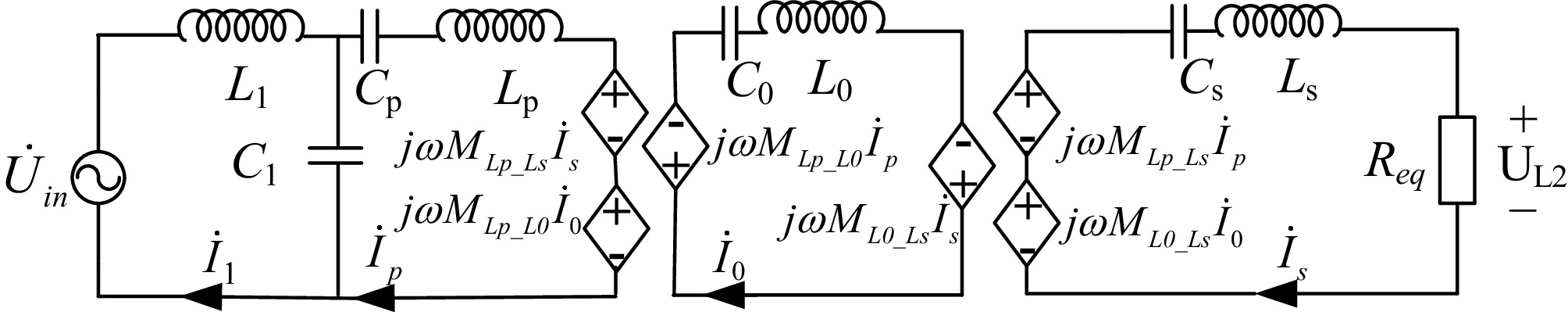
Figure 4.
Equivalent circuit with the LCC-S-S topology.
Using KVL, the following equations can be derived:
$ \left\{\begin{aligned} & {U}_{\text{in}}={I}_{1}\left(j\omega {L}_{1}+\dfrac{1}{j\omega {C}_{1}}\right)-{I}_{\text{p}}\dfrac{1}{j\omega {C}_{1}}\\ &0={I}_{\text{p}}\left(j\omega {L}_{\text{p}}+\dfrac{1}{j\omega {C}_{1}}+\dfrac{1}{j\omega {C}_{\text{p}}}\right)-{I}_{\text{1}}\dfrac{1}{j\omega {C}_{1}}-{I}_{\text{s}}j\omega {M}_{L\text{p}\_\text{}L\text{s}}-{I}_{\text{0}}j\omega {M}_{L\text{p}\_\text{}L\text{0}}\\ &0={I}_{\text{s}}\left(j\omega {L}_{\text{s}}+\dfrac{1}{j\omega {C}_{\text{s}}}\right)-{I}_{\text{p}}j\omega {M}_{L\text{p}\_\text{}L\text{s}}-{I}_{\text{0}}j\omega {M}_{L\text{0}\_\text{}L\text{s}}+{I}_{\text{s}}{R}_{\text{eq}}\\ &0=-{I}_{\text{p}}j\omega {M}_{L\text{p}\_\text{}L\text{0}}-{I}_{\text{s}}j\omega {M}_{L\text{0}\_\text{}L\text{s}}+{I}_{0}\left(j\omega {L}_{\text{0}}+\dfrac{1}{j\omega {C}_{\text{0}}}\right) \end{aligned}\right. $ (9) By substituting Eqs. (1), (2), (3), (4), and (5) into Eq. (9), one can obtain:
$ {I}_{\text{L2}}=-\dfrac{{M}_{L\text{p}\_\text{}L\text{0}}{U}_{\text{in}}}{j\omega {M}_{L\text{0}\_\text{}L\text{s}}} $ (10) $ {U}_{\text{L2}}=-\dfrac{{M}_{L\text{p}\_\text{}L\text{0}}{U}_{\text{in}}{R}_{\text{eq}}}{j\omega {M}_{L\text{0}\_\text{}L\text{s}}} $ (11) Equation (10) shows that the constant current (IL2) is dictated by MLp_L0, Uin, and ML0_Ls, which are stable without misalignment, whereas the mechanism for switching between CV and CC outputs is provided by the reconfigurable topology controlled by the switch S.
-
To corroborate the theoretical analysis and validate the switching capability between CV and CC modes, a hardware experimental prototype was fabricated, as depicted in Fig. 5. The testing bench was powered by a direct current (DC) power supply (ITECH IT6514D), and the load characteristics were simulated using a DC electronic load (ITECH IT8514B). Key operational waveforms were captured and analyzed utilizing a Tektronix MDO3024 oscilloscope.
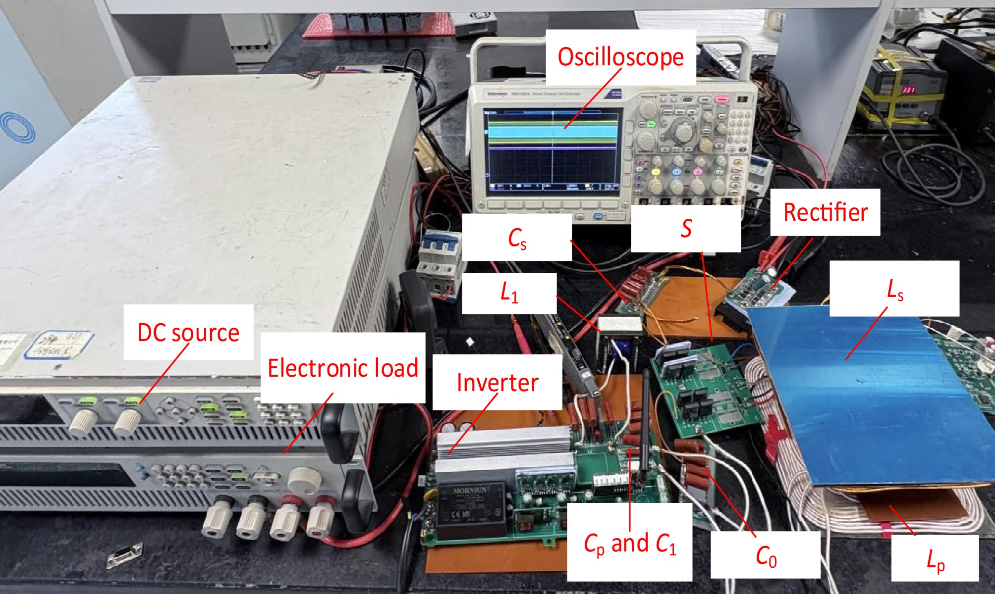
Figure 5.
Picture of the experimental setup.
The experimental apparatus, as depicted in Fig. 5, was configured with a rated input voltage of 120 V, targeting a nominal output voltage of 67 V and a charging current of 7 A. It is important to emphasize that these specific electrical parameters were selected primarily as a proof-of-concept to validate the power transfer characteristics of the proposed topology. For practical industrial deployment, the power rating possesses inherent scalability to accommodate diverse application requirements.
To minimize output fluctuations and ensure consistent power delivery during the automatic switch-over between the CV and CC outputs, a specialized parameterization framework was adopted. The design trajectory is contingent upon the ceiling of the primary coil current (Ip). Specifically, the parameters for the CV mode are resolved first; thereafter, with the primary inductance (Lp) fixed as a boundary condition, the relay and secondary coils are configured to align with the CC output demands. The system's parameters were designed by following the flowchart in Fig. 6, subject to a size limit of 20 × 20 cm for the coupling mechanism.
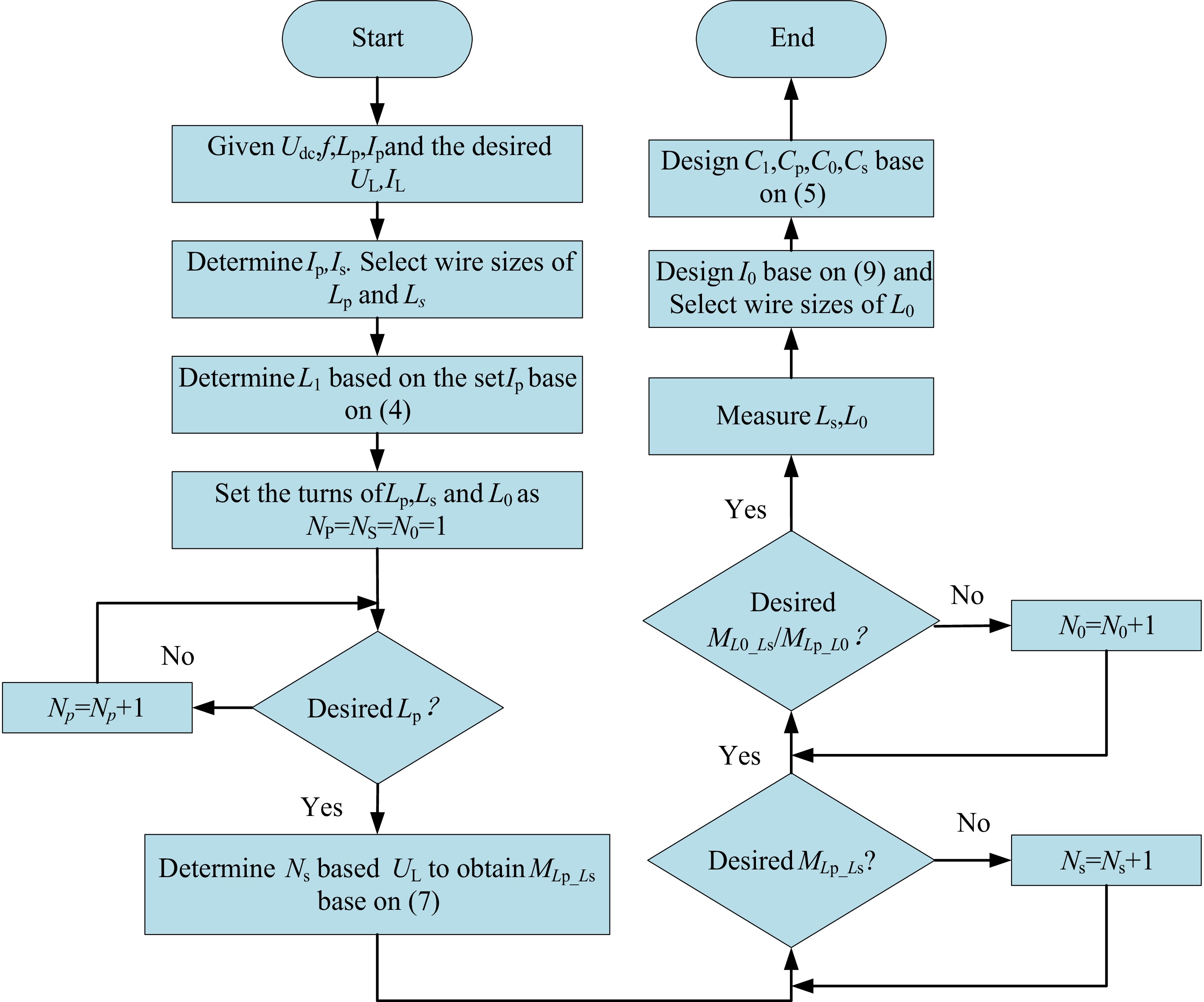
Figure 6.
Design flowchart of the system's parameters.
Step 1. Start.
Step 2. Given the initial parameters of input voltage (Udc = 120 V), frequency (f = 100 kHz), maximum primary coil current (Ip_max = 7 A), and primary coil inductance (Lp = 87.5 μH), UL and IL can be determined from Table 1 (UL = 63 V, IL = 7 A).
Step 3. The transmitter (Lp) and receiver (Ls) coils were wound using 450-strand (3 mm in diameter) and 350-strand (2.5 mm in diameter) Litz wires, respectively, selected on the basis of currents Ip and Is according to the specification table.
Step 4. In the LCC-S topology, the primary compensation inductor L1, together with the input voltage, determines the magnitude of the Ip flowing through the transmitter coil, which remains independent of the load. The design of L1 involves a critical trade-off: If L1 is too large, the resulting Ip will be insufficient, necessitating an extremely large mutual inductance M (requiring impractical coil proximity or excessive turns) to achieve the target output power (63 V/7 A); conversely, if L1 is too small, the resultant excessive Ip will impose high current stress on the MOSFETs, leading to severe coil heating or even the circuit's failure. Furthermore, it is important to note that although L1 directly influences the output voltage and current in CV mode, the output in CC mode is determined solely by the input voltage and the mutual inductance between the coils. The inductance L1_min was determined with Eq. (12).
$ {L}_{1\_ \min }=\dfrac{2\sqrt{2}{U}_{\text{dc}}}{\pi {I}_{\text{p}\_\text{max}}}\approx 35\text{ μH} $ (12) The actual measured value of the fabricated inductor L1 is 45 μH.
Step 5. Initialize the coil turns of Lp, Ls, and L0, as Np = Ns = N0 = 1.
Step 6. Determine Np. Gradually increase Np and use COMSOL software to analyze whether Lp reaches the expected value. If yes, record Np and proceed to the next step. If not, set Np = Np + 1.
Step 7. Determine Ns. Gradually increase Ns and use COMSOL software to analyze whether MLp_Ls reaches the expected value. If yes, record Np and proceed to the next step. If not, set Ns = Ns + 1. The functional correlation between the primary inductance L1 and the target output voltage UL serves as a critical metric to ascertain whether the mutual inductance MLp_Ls aligns with the theoretical design expectation.
Step 8. Determine N0. Eq. (10) defines the output current IL2 as a function of the mutual inductances MLp_L0 and ML0_Ls. Gradually increase N0 and use COMSOL software to analyze whether MLp_L0 and ML0_Ls reaches the expected value. If yes, record Np and proceed to the next step. If not, set N0 = N0 + 1. In CC mode, the output characteristics are dictated solely by the mutual inductances MLp_L0 and ML0_Ls. Consequently, the specific values for these parameters can be directly derived and validated against the target voltage and current specifications to ensure that they meet the design expectations.
Step 9. Measure Ls and L0.
Step 10. Using Eq. (9), the current I0 is calculated to determine the required wire gauge for intermediate coil L0. Subsequently, the intermediate coil (L0) is wound using a 450-strand Litz wire with a diameter of 3 mm.
Step 11. Using Eq. (5) the values of C1, Cp, Cs, and C0 are calculated.
Step 12. End.
In line with the design flowchart in Fig. 6 and the aforementioned steps, the system's parameters summarized in Table 1.
Table 1. The system's parameters.
Lp L0 Ls L1 Cp 87.5 μH 24.5 μH 84.5 μH 45 μH 61.8 nF C0 C1 Cs MLp_Ls MLp_L0 103.4 nF 46.5 nF 29.94 nF 32.5 μH 38.1 μH ML0_Ls UL IL Udc f 15.58 μH 63 V 7 A 120 V 100 kHz Np N0 Ns d 15 8 12 5 cm Switching between CV and CC modes
-
Figure 7 illustrates the dynamic voltage and current waveforms, verifying that the designed topology achieves a smooth transition mechanism independent of external control strategies. The experimental data indicate that the activation of the control switch, prompted when the system reaches its steady-state target in CV mode, successfully reconfigures the circuit for CC operation. The resulting waveforms exhibit high stability with suppressed fluctuations, thereby corroborating the system's ability to ensure a perturbation-free charging process across the mode-switching boundary.
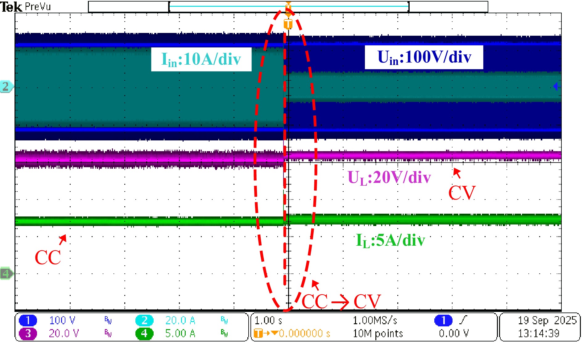
Figure 7.
Dynamic response of the system switching from CV (LCC-S) to CC (LCC-S-S) mode.
CV mode output
-
Figure 8 depicts the dynamic response of the system to a load change from 45 to 9 Ω in CV mode. This test verifies the CV output capability, showing that the output voltage deviates by only 5% (from 67.45 to 63.6 V), thereby demonstrating robust voltage regulation. At the rated operating point within the CV mode, the system is powered by a 120-V input to deliver a regulated output of 63.6 V and 7.06 A. Under this nominal condition, the measured efficiency reaches 89.6%, resulting in a total power dissipation of 52.1 W. A detailed loss analysis attributes 31.0 W to the magnetic coupling mechanism, 14.1 W to the secondary rectifier, and a minimal 7.0 W to the primary inverter, confirming that the magnetic components constitute the dominant source of loss at full load.
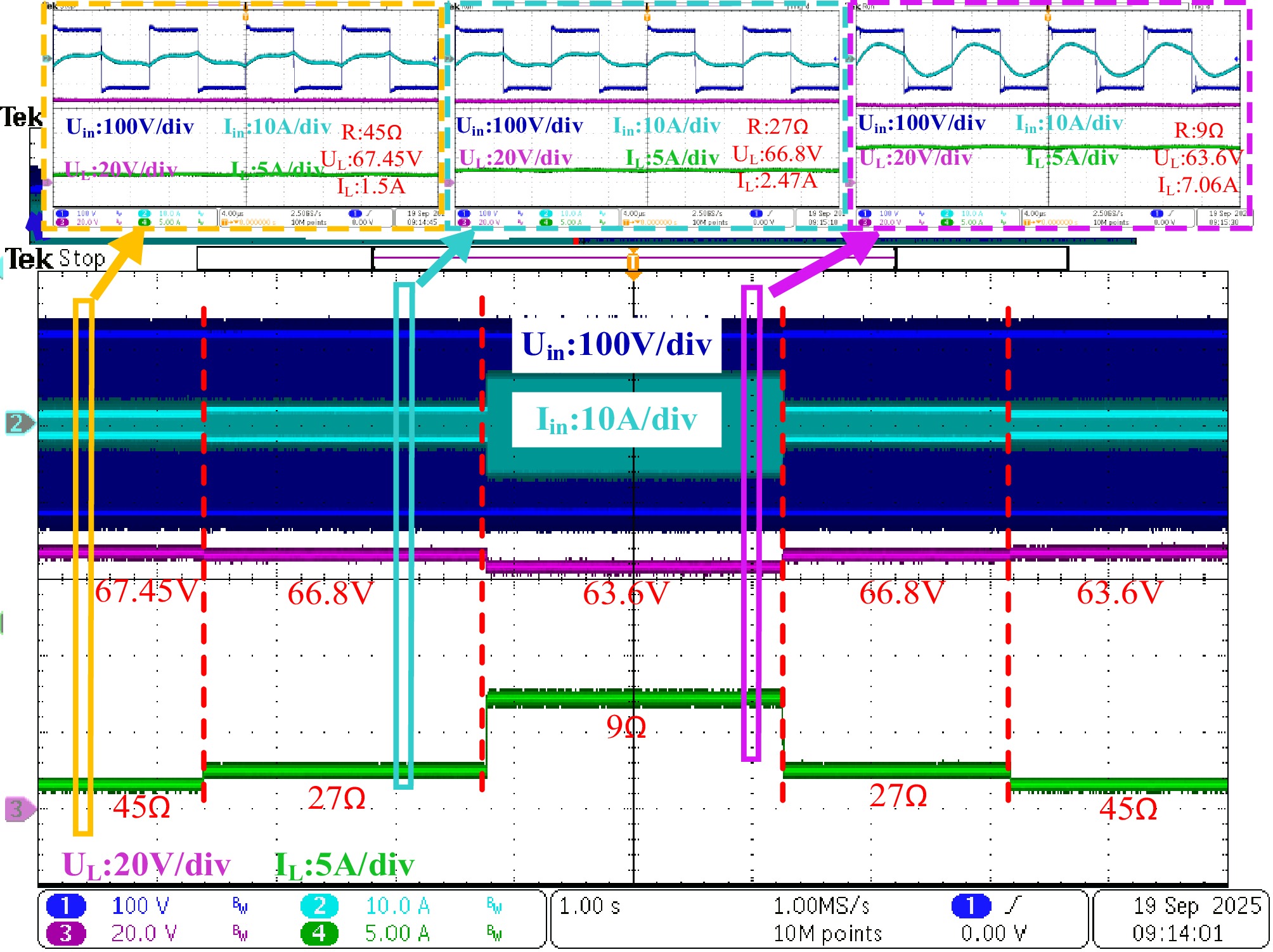
Figure 8.
Dynamic response of the system in CV (LCC-S) mode.
CC mode output
-
Figure 9 depicts the dynamic response of the system under a load variation in CC mode, where the load resistance changed from 9 to 3 Ω to validate the CC output capability. The output current varies from 7.328 to 6.906 A, with a fluctuation of only 4.6%, demonstrating the system's excellent current regulation. At the rated operating point of the CC mode, the system maintains a steady current of 6.906 A at a voltage of 62.15 V. Under this nominal condition, the experimental efficiency is measured as 88.1%, corresponding to a total power dissipation of 58.0 W. A quantitative breakdown identifies the secondary rectifier and primary inverter as contributing 13.5 and 6.9 W, respectively. However, the dominant loss component, amounting to 37.6 W, is dissipated within the magnetic coupling mechanism and the compensation network. This magnetic loss is noticeably higher than that in the CV mode, a discrepancy primarily attributed to the additional winding resistance and core losses introduced by the auxiliary compensation inductor that are essential for the CC topology.
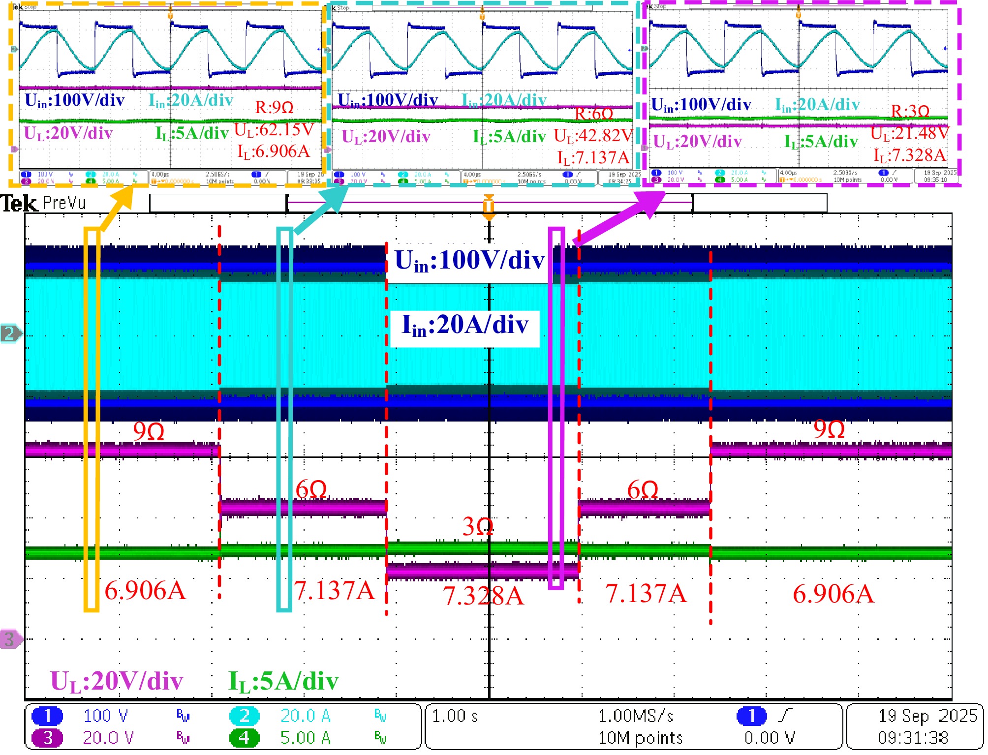
Figure 9.
Dynamic response of the system in CC (LCC-S-S) mode.
-
To comprehensively evaluate the proposed LCC-S-S system, a systematic comparison with state-of-the-art solutions reveals distinct trade-offs among efficiency, complexity, and reliability (Table 2)[15−19]. Although the hybrid reconfiguration topology and the PDM method achieve higher peak efficiencies of 94.5% and 91.55%, respectively[17,19], they introduce critical drawbacks. The hybrid switching strategy requires a complex switch matrix which significantly escalates the system's cost and failure risks[19], whereas the PDM approach relies on significantly larger coils and suffers from discontinuous power transmission, resulting in high output ripple and acoustic noise[17]. In contrast, the proposed topology offers a more optimal balance by achieving a competitive efficiency of 89.6% with minimized hardware complexity. Furthermore, unlike frequency control and phase shifting methods which rely on vulnerable wireless communication loops, posing the risks of bifurcation and signal latency[15,16], and distinct from the clamp coil method, which suffers from complex magnetic interference[18], the proposed design ensures the system's inherent stability. By operating at a fixed frequency with soft switching (ZVS) across the entire range and eliminating communication requirements, it provides a robust and economical solution that is ideal for inspection robots. Additionally, future work aims to further improve the system by incorporating wide-bandgap semiconductors silicon carbide/gallium nitride (SiC/GaN) to boost efficiency, and by utilizing adaptive frequency tuning and optimized coil structures to enhance misalignment tolerance.
Table 2. Comparison between this paper and other studies.
Ref. Method Control complexity Hardware Efficiency Main limitation and characteristic [15] Frequency control High (needs communication systems) Low (two-coil) 96.5% Risk of bifurcation and instability [16] Phase shift High (synching required) Low (two-coil) 93.59% Reactive circulating current [17] PDM High (complex system) Low (three-coil) 91.55% High output ripple and acoustic noise [18] Clamp coil Low (passive) High (three-coil) 90.2% Complex cross-coupling issues [19] Hybrid switch Medium (multi-switch) Very high 94.5% High cost and low reliability Proposed LCC-S-S Very low (open-loop) Moderate 89.6% Optimal balance: Robust and cost-effective -
This paper presents a wireless power transfer system suitable for inspection robots. Through an analysis of multi-stage topologies and the circuits' characteristics, key parameters of the resonant network and the loosely coupled transformer were designed. The system enables natural switching between CC (LCC-S-S) and CV modes (LCC-S) via a single switch in response to load variations, without requiring additional control circuits or communication mechanisms, offering advantages such as a simple structure and a straightforward control strategy. A 63-V, 7-A experimental prototype with a peak efficiency of 89.6% demonstrated that the output voltage remains essentially constant in CV mode, with a fluctuation within 5% under significant load variations. Similarly, in CC mode, the output current remains stable, with only 4.6% fluctuation under large load changes, whereas the system maintains a stable voltage and current output during CV–CC mode transitions. The findings provide a feasible solution for implementing highly reliable wireless charging systems under varying load conditions.
-
The authors confirm their contributions to the paper as follows: study conception and design: Xie Y, Zheng H; data collection: Wang Z, Zuo Z; analysis and interpretation of results: Xie Y, Zheng H; draft manuscript preparation: Zuo Z. All authors reviewed the results and approved the final version of the manuscript.
-
The datasets generated during and/or analyzed in the current study are available from the corresponding author on reasonable request.
-
This work was supported in part by the Fundamental Research Funds for the Central Universities under Grant 2024CDJGF-015 and in part by Project of Sichuan and Chongqing Science and Technology Innovation Cooperation Plan under Chongqing's Technological Innovation and Application Development Initiative (CSTB2024TIAD-CYKJCXX0002) and Chongqing New Youth Innovation Talent Program (CSTB2024NSCQ-QCXMX0009).
-
The authors declare that they have no conflict of interest.
- Copyright: © 2026 by the author(s). Published by Maximum Academic Press, Fayetteville, GA. This article is an open access article distributed under Creative Commons Attribution License (CC BY 4.0), visit https://creativecommons.org/licenses/by/4.0/.
-
About this article
Cite this article
Xie Y, Zheng H, Wang Z, Zuo Z. 2026. A magnetic coupling-based wireless power transfer system with automatic constant current–constant voltage charging. Wireless Power Transfer 13: e018 doi: 10.48130/wpt-0026-0008 

A magnetic coupling-based wireless power transfer system with automatic constant current–constant voltage charging
- Received: 19 November 2025
- Revised: 04 January 2026
- Accepted: 23 January 2026
- Published online: 05 June 2026
Abstract: This paper presents a novel LCC primary compensation + series–series (S–S) secondary compensation multi-stage compensation topology to meet the requirement for self-adaptive switching between constant current (CC) and constant voltage (CV) modes in low-power wireless charging systems for inspection robots. A key advantage of the proposed topology is its ability to provide stable CC and CV outputs as required through a simple topological reconfiguration, without relying on additional control algorithms, which substantially simplifies the control logic. To verify the design's feasibility, an experimental platform targeting 63 V/7 A was constructed. Performance tests indicate that in CV mode, the system maintains a stable output of 67 V with a fluctuation of only 5%. Correspondingly, in CC mode, it delivers a stable current of 7 A with a mere 4.6% fluctuation. These results conclusively validate the effectiveness and rationality of the proposed LCC-S-S topology and its parameter design.