


-
In recent years, significant advancements in solar cell technology have transformed the photovoltaic industry, with perovskite solar cells emerging as the fastest-growing technology[1−10]. The exceptional properties of perovskite absorber layer-based solar cells, such as a high absorption coefficient, low-temperature fabrication process, high diffusion length, high carrier mobility, and tunable bandgap, making them the most promising photovoltaic cells. The low-cost fabrication process of perovskite solar cells also contributes to their high-power conversion efficiency (PCE). Formamidinium, methylammonium, and lead in the B cation site and cesium in the A cation site, with halogens (iodine, bromine) in the X-anion site, have been the most successful combination of metal halide-based perovskite solar cells in the ABX3 structure[11]. Extensive research has been carried out to enhance the photovoltaic performance of CH3NH3PI3-based perovskite solar cells[12−17]. Nevertheless, the use of perovskite solar cells is currently limited by the toxic nature of lead and device instability in the air[18−20]. Researchers are therefore exploring new, advanced, lead-free perovskite materials to overcome these challenges. A recent discovery of lead-free MASnI3-based perovskite material, due to its non-toxicity and earth abundance, could be used instead of CH3NH3PbI3[21,22].
Various electron transport layers (ETLs) have been employed with the MASnI3-based absorber layer, such as CeO2, ZnO, CdS, and TiO2, to enhance device performance[23−25]. However, the oxidation of Sn2+ to Sn4+ when exposed to air, resulting in the formation of MAI and SnO2, has been observed in previous studies[26]. In PSCs, titania and Spiro-OMeTAD are typically used as the electron and hole transport layers, respectively. However, the high-temperature fabrication process of the titania layer significantly affects the stability and performance of the solar cell. Furthermore, the output efficiency decreases with the evaporation of Spiro-OMeTAD additives. The SnO2 is widely used as an electron transport layer (ETL) in perovskite solar cells due to its high electron mobility, good optical transparency, high electron mobility, chemical stability, low-temperature processing, optical transparency, thermodynamic stability and compatibility with tin-based perovskites. These properties make it an excellent candidate for efficient charge extraction and minimal energy loss at the interface. SnO2 is an exceptional material due to its superior optoelectrical properties, among a range of available metal oxides such as TiO2, SrTiO3, ZnO, In2O3, Zn2SnO4, and WO3. Using SnO2 as ETL improves the absorber layer band alignment and enhances the stability of the devices. Spiro-OMeTAD remains the most commonly used hole transport layer. However, the performance of PSCs can be adversely affected by the interaction of Spiro-OMeTAD with humidity, UV light, and moisture. On the other hand, GaAs possesses higher carrier mobility, is less sensitive to overheating due to its wider bandgap, and is lightweight and flexible, making it a promising material for use as a hole transport layer (HTL). Several studies have reported high PCEs for PSCs utilizing different materials for the charge transport layers, such as IGZO as an electron transport layer (ETL) and Cd0.5Zn0.5S as a hole transport material (HTM) with a light-harvesting layer of MASnI3, resulting in a PCE of 23.86%. Additionally, a modeling study using mixed halide MASnI3 as the absorber layer and CuO as the HTL showed an efficiency of 24.14%[27]. To achieve better photovoltaic parameters, it is important to explore suitable substitutes for the commonly used charge transport layers. Moreover, Pb-based PSCs are hazardous to the environment due to the toxicity of Pb. Therefore, it is crucial to discover a Pb-free absorber layer along with new inorganic charge transport layers to improve the photovoltaic parameters. With these aspects in mind, this paper reports a comprehensive investigation of a Sn-based device configuration with SnO2 and GaAs as the ETL and HTL, respectively. The characteristics of the photovoltaic device can be influenced by temperature and interface defect density, so the proposed solar cell's performance is examined at different temperatures and interface defect densities to determine the best possible device configuration. Furthermore, this work can assist in refining the PCE of the photovoltaic device by identifying the influence of the solar cell's functional layer thicknesses.
Tin-halide-based perovskite solar cells have emerged as a promising alternative to their lead-based counterparts, driven by the need for more environmentally friendly and non-toxic materials. As both tin and lead belong to Group 14 of the periodic table, tin-based perovskites offer a similar crystal structure and optoelectronic properties, making them a viable candidate for efficient photovoltaic applications. However, achieving high performance in tin-halide perovskite solar cells remain challenging due to issues like the rapid oxidation of tin (from Sn2+ to Sn4+) and the presence of deep trap states, which contribute to lower device efficiency and stability compared to lead-based perovskites. Despite these challenges, recent advancements in material engineering, device architecture, and interface optimization have led to significant improvements in the PCE of tin-based perovskite solar cells, marking a critical step toward their potential commercialization[28].
Incorporating polyvinyl alcohol (PVA) into SnO2 electron transport layers significantly improves perovskite solar cell performance. The SnO2-PVA ETL enhances carrier transport and perovskite film quality, achieving a maximum PCE of 23.73% and excellent stability, retaining 90% of initial performance after 1,000 h. The methoxyamine hydrochloride (MOACl) as a modifier for tin dioxide (SnO2) electron transport layers (ETLs) in PSCs improves the film quality of SnO2, leading to enhanced electrical conductivity, electron mobility, and perovskite crystallization[29]. The modified SnO2-ETL PSCs exhibit improved performance, with a PCE of 24.34%, which is an increase of 2.67% from the original value. Another novel approach to improve the performance of PSCs is modifying the SnO2 electron transport layer (ETL) with a non-ionic polymer, polyacrylamide (PAM)[30]. The modification effectively inhibits the aggregation of SnO2 nanoparticles, resulting in homogeneous and dense perovskite films with improved interfacial contact contributing to a higher PCE of 21.61%. A novel strategy to enhance the efficiency and stability of PSCs involves using a phosphorus hetero-phenanthrene flame retardant called DOPO as a surface modifier for the SnO2 electron transport layer (ETL)[31]. This approach helps passivate surface defects on the SnO2 ETL, improving carrier transport efficiency and the crystalline quality of the perovskite layer. The optimized PSCs achieved a significant increase in photoelectric PCE from 19.74% to 22.81%. Another study presented a ligand-assisted strategy to enhance the performance of PSCs by modifying the tin dioxide (SnO2) electron-transporting layer (ETL) with oxalic acid (OA)[32]. As a result, the modified PSCs achieved a high photo-conversion efficiency of 22.68%. The zirconium acetate stabilized tin dioxide (ZAS) quantum dots were utilized as the electron transport layer (ETL)[33]. The ZAS ETL passivated defects at the perovskite surface, resulting in better energy level alignment and efficient electron transport, and achieved a PCE of 21.13%.
In continuation of these efforts, Deepika et al.[34] employed the SCAPS-1D simulation tool to demonstrate the potential of tin-based perovskite solar cells as a more environmentally friendly alternative to traditional lead-based PSCs. The study revealed that a maximum PCE of 30.33% could be achieved with a device configuration of FTO/SnO2/FASnI3/CuI/Au, optimizing the active layer thickness at 450 nm, with an interfacial defect density (Nt) of 1 × 1013 cm−3 at a device temperature of 300 K. Similarly, another study focused on methylammonium tin iodide (MASnI3) based PSCs, simulated using SCAPS-1D software, where an ITO/CeO2/MASnI3/CuCrO2/Au structure achieved a PCE of 26.60%[35]. In efforts to replace lead (Pb) in methylammonium lead iodide (MAPbI3) perovskite solar cells, researchers have explored Bi-doped PSCs, fabricated under ambient conditions using a sandwich structure to reduce toxicity and improve stability. Although the efficiency of Bi-doped PSCs (5.1%) was lower than that of MAPbI3-based PSCs (6.7%), they demonstrated significantly better stability, retaining 90% of their original efficiency after 120 h and continuing to function after 35 d[36]. Further advancements were made in the study of lead-free perovskite solar cells by comparing rubidium-tin-chloride (RbSnCl3) and rubidium-lead-bromide (RbPbBr3) using density functional theory (DFT) and the SCAPS-1D simulator. The heterostructure Al/FTO/SnS2/(RbPbBr3 and RbSnCl3)/Au achieved PCEs of 29.75% for RbPbBr3 and 33.61% for RbSnCl3, demonstrating that RbSnCl3 offers a promising lead-free alternative with superior efficiency metrics[37]. Moreover, a recent study[38] employed numerical simulations to investigate the impact of different Zn doping ratios (0%, 2%, 5%, and 10%) on the performance of FASnI3-based PSCs. The results indicated that a 5% Zn doping ratio (Zn-5) provided the best performance, with a PCE of 11.49% at an absorber layer thickness of 400 nm. Another study[39] explored the use of bismuth (Bi) as a replacement for lead (Pb) in the absorber material, investigating the impact of various configurations on solar cell performance. It was found that the configuration using FTO/CdS/CH3NH3BiI3/MoS2/Pt achieved an efficiency of 26.60%, a current density of 32.02 mA/cm2, an open circuit voltage of 0.974 V, and a fill factor (FF) of 85.24%. In a related study, Naik et al.[40] explored the potential of CH3NH3SnI3-based solar cells as efficient, lead-free alternatives in photovoltaic technology, identifying an optimal architecture of Ag/PFN-Br/CH3NH3SnI3/PEDOT/Pt, which achieved a PCE of 31.11%. Further research has also concentrated on the performance of lead-free perovskite solar cells, specifically in single-layer and bilayer structures. Using SCAPS-1D software, device parameters such as thickness, doping concentration, defect density, and series-shunt resistance were optimized. The results showed that the bilayer structure with a CH3NH3SnBr3/CIGS layer achieved a higher PCE (22.68%) compared to the single-layer structure (20.58%)[41].
-
To analyze and optimize the performance of the device, the SCAPS-1D software is utilized, which employs 1-dimensional equations for simulation. The input spectrum is based on the standard AM 1.5 solar spectrum irradiance. The software employs continuity equations (of electron and hole), and the Poisson equation, to compute the output photovoltaic parameters.
ddx{ε(x)ddxψ}=q[p(x)−n(x)+N+D(x)+N−A(x)pt(x)−nt(x)] (1) −iJddxjp+Rp(x)−G(x)=0 (2) −ijddxjn+Rn(x)−G(x)=0 (3) The equations used to model the behavior of the photovoltaic device are based on several parameters. The elementary charge is represented by 'q', the static relative permittivity is εs, and the hole-density is represented by 'p'. Similarly, 'n' represents the electron density, (ND+) stands for the density of ionized donors, (NA−) for the density of ionized acceptors, and Ndef represents the density of possible defects (either donor or acceptor). The rate of partial increase in hole (electron) is represented by ∂p/∂t (∂n/∂t). The hole current density is denoted by Jp, while Jn represents the electron current density. The electrostatic potential is represented by ψ. The net recombination rate for holes (electrons) is denoted by Up(Un), while the generation rate of electron-hole pairs is represented as 'G'.
The SCAPS software uses continuity equations (of electron and hole). By solving the continuity equations, it can predict how modifications to the material properties, device structure, or operating conditions will impact carrier behavior and, consequently, device performance. They are essential for understanding the behavior of charge carriers under various conditions, guiding the design and optimization of semiconductor devices to achieve desired characteristics such as efficiency, speed, and sensitivity. SCAPS-1D also uses the Poisson equation to calculate the output photovoltaic parameters. It determines the spatial distribution of the electric field within the photovoltaic device. This electric field drives the separation of photo-generated electron-hole pairs, which is essential for generating current in a solar cell. It calculates the photovoltaic parameters by modeling the electric potential and electric field within the device. These fields are critical for the separation and collection of charge carriers, directly impacting key photovoltaic parameters such as open-circuit voltage, short-circuit current, fill factor, and overall efficiency. Poisson's equation can predict how changes in the material properties, device structure, and operating conditions will influence the performance of photovoltaic devices[42−44].
The SCAPS software is a Windows-based program that was developed at the Department of Electronics and Information Systems (ELIS), University of Ghent, Belgium[45]. It boasts several key features, including the ability to incorporate up to seven semiconductor layers, grade virtually all physical parameters, estimate carrier transport mechanisms, steady state band diagrams, and recombination summaries, and study changeable temperature, voltage bias, and illumination options. Additionally, the software can calculate Q-V characteristics, spectral response, concentrations, C-V, C-F, J-V, and current at a given point. It can also simulate I-V solar cells by modifying absorption coefficient and provide a single or collection of values, immediate and final values, graphs, and other essential data.
The data obtained from SCAPS-1D for a single cell is incorporated as input in the PVSyst package for simulation of a solar module. PVSyst, a software tool designed for the planning, simulation, and assessment of solar photovoltaic systems, integrates various input parameters including system setup, location-specific weather data, and module specifications to create a detailed model of the solar PV system. Using this model, PVSyst predicts the system's energy output and provides key metrics such as annual energy generation, system efficiency, and capacity factor. Additionally, the software conducts shading analysis, considers inverter efficiency, and factors in other system losses to offer an accurate representation of its performance. PVSyst boasts an extensive database containing meteorological data for over 30,000 locations worldwide, enabling precise simulation of solar energy production under diverse weather conditions.
The energy band gap of SnO2 (3.6 eV) is chosen to ensure that it does not absorb visible light, thereby allowing maximum light to reach the perovskite absorber layer which is ultimately responsible for charge carriers generation for efficient working of solar cells. The high electron mobility of SnO2 (100 cm2/Vs) is selected to facilitate efficient electron transport and reduce recombination losses, which is critical for improving the overall device efficiency. The thickness of SnO2 is set at 0.044 μm to balance between effective charge transport and minimizing recombination losses. The thickness is optimized to ensure that it provides a good interface with the perovskite layer. A thinner layer would lead to reduced charge extraction, while a thicker layer would increase recombination losses. The carrier density 2.2 × 1018 cm−3 is chosen to ensure a reasonable charge extraction rate while minimizing recombination losses.
The absorber material CH3NH3SnI3 is selected as the perovskite absorber due to its suitable band gap (1.35 eV) for efficient light absorption across the visible spectrum. This material has been shown to provide a good balance between optical absorption and charge carrier mobility. The choice of CH3NH3SnI3 also aligns with the growing interest in developing lead-free perovskite solar cells, addressing environmental and health concerns associated with lead-based perovskites. The absorber layer thickness is set at 4.6 μm. This value is selected to optimize light absorption while maintaining efficient charge carrier collection. The 4.6 μm thickness for the MASnI3 perovskite absorber is based on the need to achieve a balance between light absorption and recombination losses. A thinner layer would lead to reduced light absorption, while a thicker layer would increase recombination losses. The bandgap of 1.35 eV is based on experimental values and literature reports. The carrier density of 1 × 1018 cm−3 is chosen to account for the intrinsic defects and impurities in the perovskite material. The selection of parameters like electron affinity, relative permittivity, and thermal velocities are based on well-established values from experimental data and previous simulation studies. These parameters are chosen to closely mimic real device conditions and ensure the accuracy of the simulation results[46,47].
-
The proposed solar cell composition comprises distinct layers, each with specific roles crucial for efficient photovoltaic performance. Indium tin oxide (ITO), as the top layer, serves as a transparent conductive material, allowing incident light to penetrate while facilitating the extraction of generated charge carriers. Tin oxide (SnO2), functioning as the ETL, promotes efficient electron extraction from the perovskite absorber layer to the external circuit, minimizing carrier recombination and enhancing device stability.
The CH3NH3SnI3 layer, composed of organometal halide perovskite, acts as the absorber layer and is pivotal for light absorption and electron-hole pair generation. Perovskite materials exhibit exceptional light-harvesting capabilities and high carrier mobility, making them promising candidates for photovoltaic applications. Gallium Arsenide (GaAs) serves as HTL, facilitating the efficient transport of photo-generated holes from the perovskite layer to the external circuit. GaAs possess superior electronic properties, including high carrier mobility and low recombination rates, which contribute to enhanced charge extraction and overall device efficiency.
Finally, Molybdenum (Mo) serves as the back contact layer, providing a low-resistance pathway for the extraction of photo-generated electrons to the external circuit. Mo's compatibility with other layers and its robust electrical properties make it an ideal choice for ensuring efficient charge collection and minimizing energy losses.
The proposed solar cell composition holds significant importance in advancing photovoltaic technology. By leveraging the unique properties of each layer, this composition aims to maximize light absorption, charge carrier extraction, and device efficiency. The integration of transparent conductive oxide ITO and efficient electron transport layer SnO2 enables enhanced light transmission and charge extraction, respectively. Furthermore, the utilization of perovskite absorber materials offers exceptional light-harvesting capabilities and high carrier mobility, promising high efficiency and cost-effectiveness. Additionally, GaAs and Mo layers contribute to efficient charge transport and collection, further optimizing device performance. Overall, this proposed solar cell composition represents a strategic combination of materials tailored to achieve superior photovoltaic performance, laying the foundation for the development of next-generation solar cells with enhanced efficiency and stability.
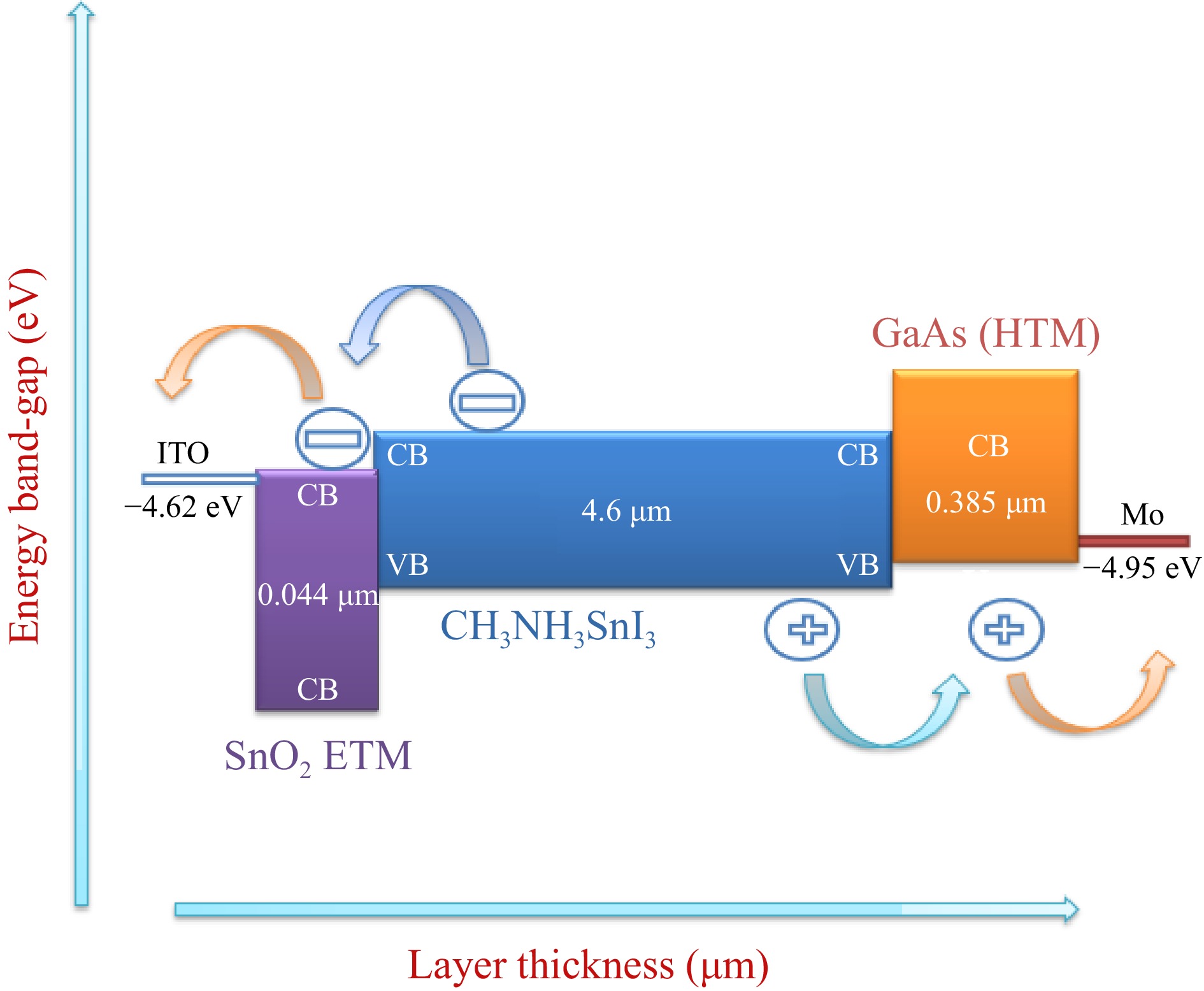
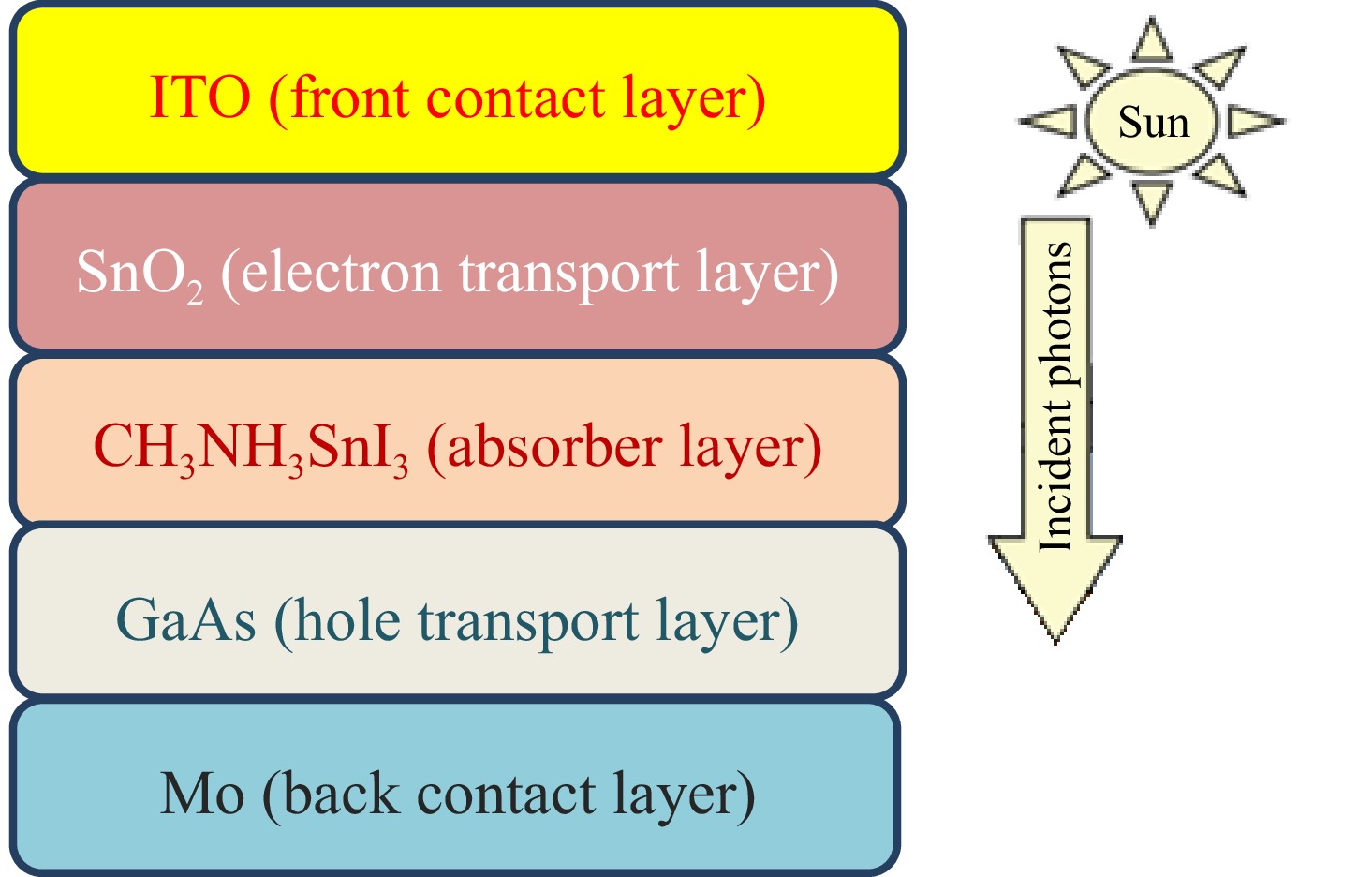
The performance of a solar cell depends greatly on the device structure. The proposed structure of the tin-based perovskite solar cell is depicted in Fig. 1. The device configuration employed in this study consists of ITO/SnO2/CH3NH3SnI3/GaAs/Mo. Sunlight photons penetrate through the indium tin oxide (front contact layer), while SnO2 (electron transport layer) allows electrons to move from CH3NH3SnI3 (perovskite absorber layer) to ITO. The absorber layer serves as an intermediary layer between the HTL and ETL. When photons interact with the absorber layer, they produce electron-hole pairs. These photoelectrons are transported toward the front contact layer by the SnO2-based ETL, while photo-generated holes are transported to the back contact layer by the HTL. An electric current is generated by extracting electrons through the external circuit via ITO.
Figure 1 illustrates the standard n-i-p structure of the proposed tin-based perovskite solar cell configuration, which was studied in detail during this research work. Molybdenum (Mo) is employed as the back contact metal. The simulations were performed using standard parameters with AM 1.5 G solar spectrum under 100 mW/cm2 solar power at 300 K temperature. An efficiency of 27% has already been reported[48] with MASnI3 as the absorber layer. Furthermore, various experimental studies have shown that the device performance is greatly influenced by the morphology of the perovskite active layer, which affects diffusion length and charge carrier lifetime[49,50].

Figure 1.
Schematic structure of proposed device ITO/SnO2/CH3NH3SnI3/GaAs/Mo.
-
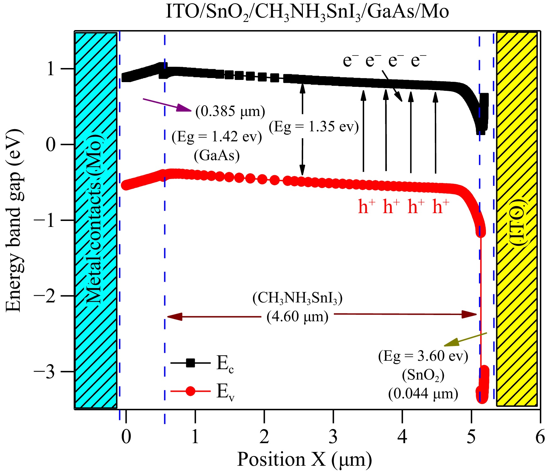
Figure 2 illustrates that the conduction band (CB) level of the SnO2-based ETL material is lower than that of the CH3NH3SnI3-based absorber material. This difference in CB levels is crucial for the flow of electrons from a higher energy level to a lower energy level. Likewise, the valence band (VB) of the HTL material should be higher than that of the absorber material to conduct holes from the absorber material to the HTL. To transfer electrons/holes from the electron/hole transport layer to the respective metal contact, it is necessary to adjust the conduction/valence band minimum/maximum of the electron/hole transport layer near to the indium/molybdenum metal contact. The device structure depicted in Fig. 2 fulfills the essential requirements for electron/hole transportation between functional layers of the proposed solar cell. Furthermore, the SnO2/CH3NH3SnI3 interface shows that the CB of SnO2 is slightly lower than that of CH3NH3SnI3. This built-in electric field enhances the flow of electrons from the absorber layer to the ETL. Similarly, the CH3NH3SnI3/GaAs interface shows that the VB of HTL is slightly adjusted above that of the absorber layer, facilitating the movement of holes from the absorber layer to the HTL. Consequently, the efficiency of the device increases, and energy losses decrease.
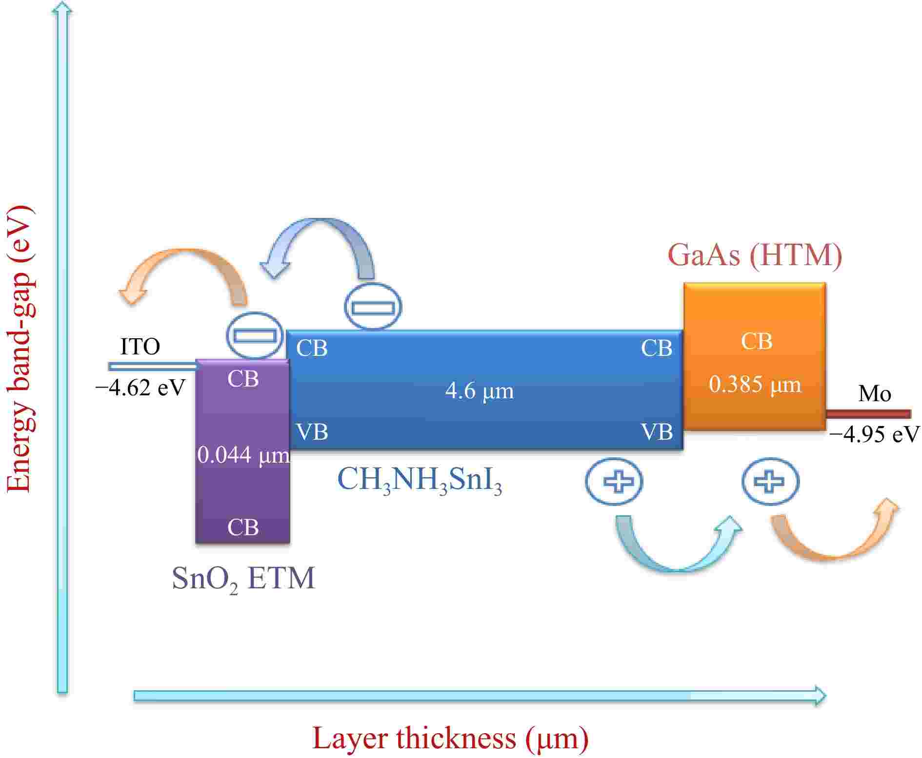
Figure 2.
Energy band-gap versus layer thickness of Perovskite solar cell.
-
Figure 3 depicts the energy band arrangement in the proposed solar cell. The difference between the conduction band (CB) level of perovskite material and ETL is termed as conduction band offset (CBO). A negative CBO is observed when the CB level of perovskite material is higher than that of ETL. In this case, an energy cliff is formed at the perovskite/ETL interface. On the contrary, if the CB level of the absorber material is lower than the CB of ETL, a positive CBO is generated which results in the formation of an energy spike. Photo-generated electrons flow smoothly without encountering any energy cliff. Although the activation energy for charge carrier recombination is lower than the absorber band gap[51,52], it becomes equivalent to the active layer band gap at the ETL/perovskite junction due to the energy spike. If the activation energy is higher than that computed by the energy cliff, it can improve the device performance. The impact of the energy spike on the charge carrier recombination rate is observed within a small range of motion for photo-generated electrons[53].

Figure 3.
Schematic diagram of valence and conduction band of ITO/SnO2/CH3NH3SnI3/GaAs/Mo solar cell.
-
In this study, a perovskite solar cell (PSC) with a methyl ammonium tin iodide absorber layer was modeled and simulated using SCAPS-1D software. An essential investigation was conducted to identify an efficient and stable electron transport layer (ETL) for CH3NH3SnI3 based PSC. The input parameters required for simulations are presented in detail in Table 1. The results were then illustrated in both graphical and tabular form. The SnO2-based ETL was utilized to transport the photoelectrons generated by the absorber layer towards the front contact layer. In a similar way, photo-generated holes were transported to the back contact layer by the hole transport layer (HTL). The extraction of electrons by the external circuit through ITO generated an electric current. The material parameters and interface defect details are given in Table 2.
Table 1. Material parameters of HTLs, absorber layer and ETL.
Material parameters SnO2
(ETL)MASnI3
(absorber layer)GaAs
(HTL)X (μm) 0.044 Arbitrary 4.60 Arbitrary 0.385 Arbitrary Eg (eV) 3.60 1.35 1.42 χ (eV) 4.000 4.17 4.070 ε (relative) 9.000 6.500 12.900 Nc (cm−3) 2.200E+18 1.000E+18 2.200E+18 Nv (cm−3) 1.800E+19 1.000E+19 1.800E+19 Ve (cms−1) 1.000E+7 1.000E+7 1.00E+7 Vh (cms−1) 1.000E+7 1.000E+7 1.00E+7 μe (cm2V−1-s1) 1.000E+2 1.600E+0 8.500E+3 μh (cm2V−1-s1) 2.500E+1 1.600E+0 4.000E+2 ND (cm−3) 1.000E+18 0.0 0.0 NA (cm−3) 0.0 3.200E+15 1.000E+11 Nt (cm−3) 1.000E+15 − 1.000E+14 Nt (cm−3) 5.642E+15 − Table 2. Material parameters of HTLs/ CH3NH3SnI3 interface defects and CH3NH3SnI3/ C60 interface defects.
Material parameters CuI/CH3NH3SnI3
interfaceCuSCN/CH3NH3SnI3
interfaceCH3NH3SnI3/C60
interfaceDefect type Neutral Neutral Neutral Capture cross section for (n,p) (cm−2) 1 × 10⁻¹⁹ 1 × 10⁻¹⁹ 1 × 10⁻¹⁹ Energy distribution Single Single Single E- level w.r.t Ev (above Ev, Ev) 0.6 0.6 0.6 Total density (cm−3) 1 × 10¹³ 1 × 10¹³ 1 × 10¹³ Impact of perovskite layer thickness
-
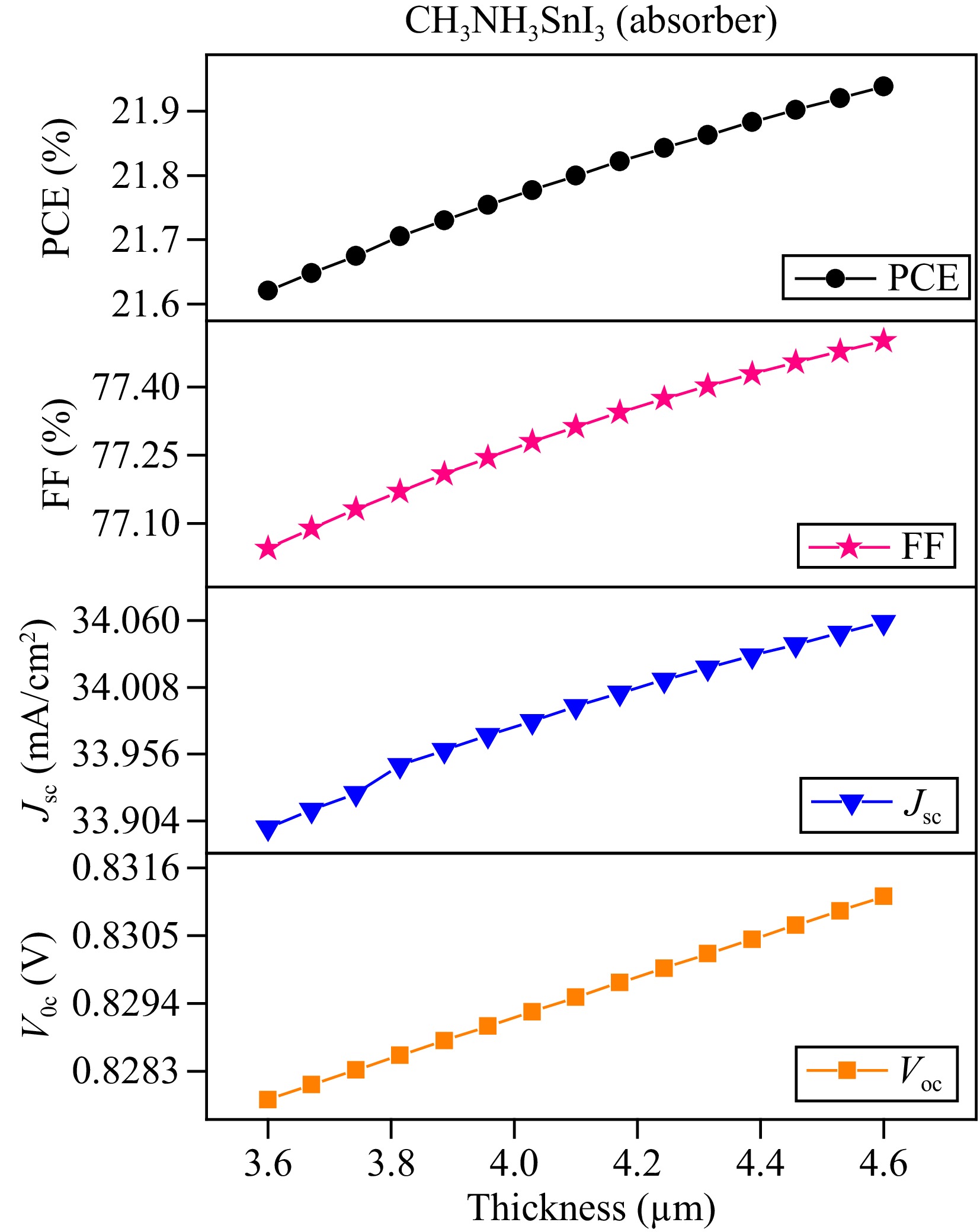
Figure 4 presents the changes in characteristic parameters of the solar cell as a function of the thickness of its active layer. The simulations were carried out using the SCAPS-1D software at 300 K temperature and the standard AM 1.5 G light spectrum. The performance of the designed solar cell was evaluated within the absorber thickness range of 3.6 to 4.6 μm. It is observed that all the photovoltaic parameters increase as the thickness of the perovskite (absorber) layer increases. At a thickness of 3.6 μm, the open-circuit voltage value was recorded as 0.827 V, which increases to 0.831 V at 4.6 μm thickness. Similarly, current density Jsc increases with absorber thickness up to 4.6 μm and then reaches saturation. Jsc values of 33.898 mA·cm−2 and 34.058 mA·cm−2 were calculated at an absorber thickness of 3.6 and 4.6 μm, respectively. The increase in photon absorption with an increase in absorber layer thickness at larger values of the wavelength is responsible for the increase in Jsc. Furthermore, both fill factor and PCE exhibit an increasing trend, i.e., 77.044% to 77.501% and 21.620% to 21.938%, respectively. However, optimum values are observed in all parameters after 4.6 μm absorber thickness due to charge carrier recombination in the active layer before reaching the metal electrodes. Therefore, the optimized thickness of the active layer is selected as 4.6 μm to control the charge carrier recombination rate and to achieve an optimized device performance. The optimized thickness of the absorber material MASnI3 is fixed at 4.6 μm for future research work.
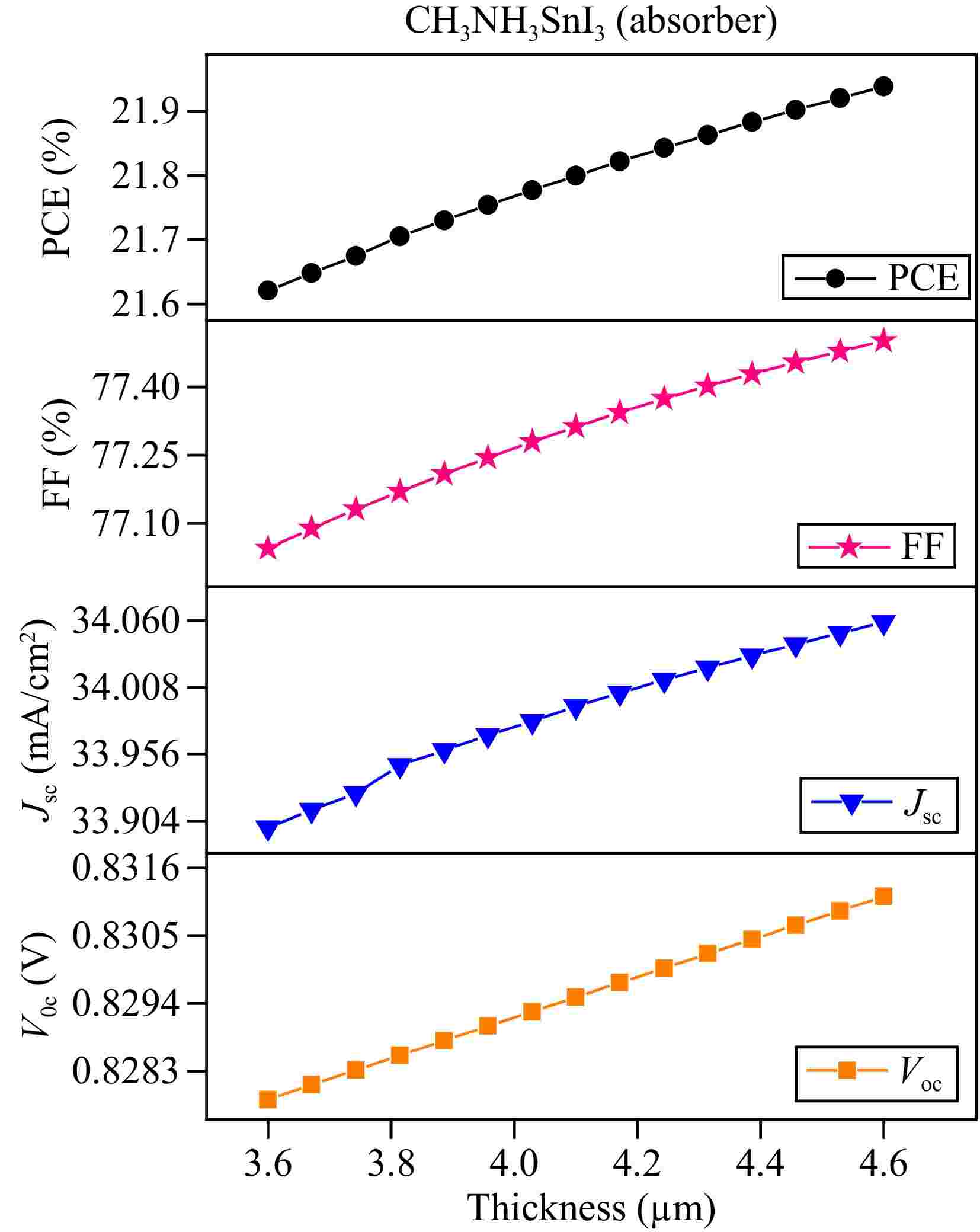
Figure 4.
Effect of absorber thickness on electrical parameters.
The increasing trend in electrical parameters (Voc, Jsc, FF, and PCE) with the variation of absorber material CH3NH3SnI3 layer thickness from 3.6 to 4.6 μm is primarily driven by enhanced photon absorption and charge carrier dynamics. With the fact absorber layer thickens, the material captures a greater proportion of incident light, leading to higher Jsc value due to increased carrier generation. Thicker layers offer more volume for absorbing photons, which generates a higher density of electron-hole pairs, thus boosting the current density. The rise in Voc may be attributed to reduced recombination losses. A thicker absorber reduces the likelihood of carriers recombining before reaching the electrodes, enabling the accumulation of more photo-generated charge carriers, which increases the built-in potential and leads to higher Voc. Additionally, the longer carrier lifetimes in thicker layers contribute to more effective separation of charge carriers, further supporting Voc enhancement. For FF, the improved charge transport in thicker layers helps minimize resistive losses, allowing a more efficient extraction of photo-generated carriers. This leads to better charge collection and an overall improvement in device performance. Thicker layers also reduce surface recombination, which otherwise degrades FF. Finally, the overall increase in PCE results from the combined improvements in Jsc, Voc, and FF. However, the trend did not saturate because, at even greater thicknesses, the increased series resistance and potential for bulk recombination would begin to counterbalance these gains. Excessively thick layers can lead to transport bottlenecks, diminishing carrier collection and introducing resistive losses, which is why higher thickness values were not explored further. The trade-off between absorption and transport efficiency becomes crucial in optimizing the device structure.
Effect of electron transport layer thickness
-
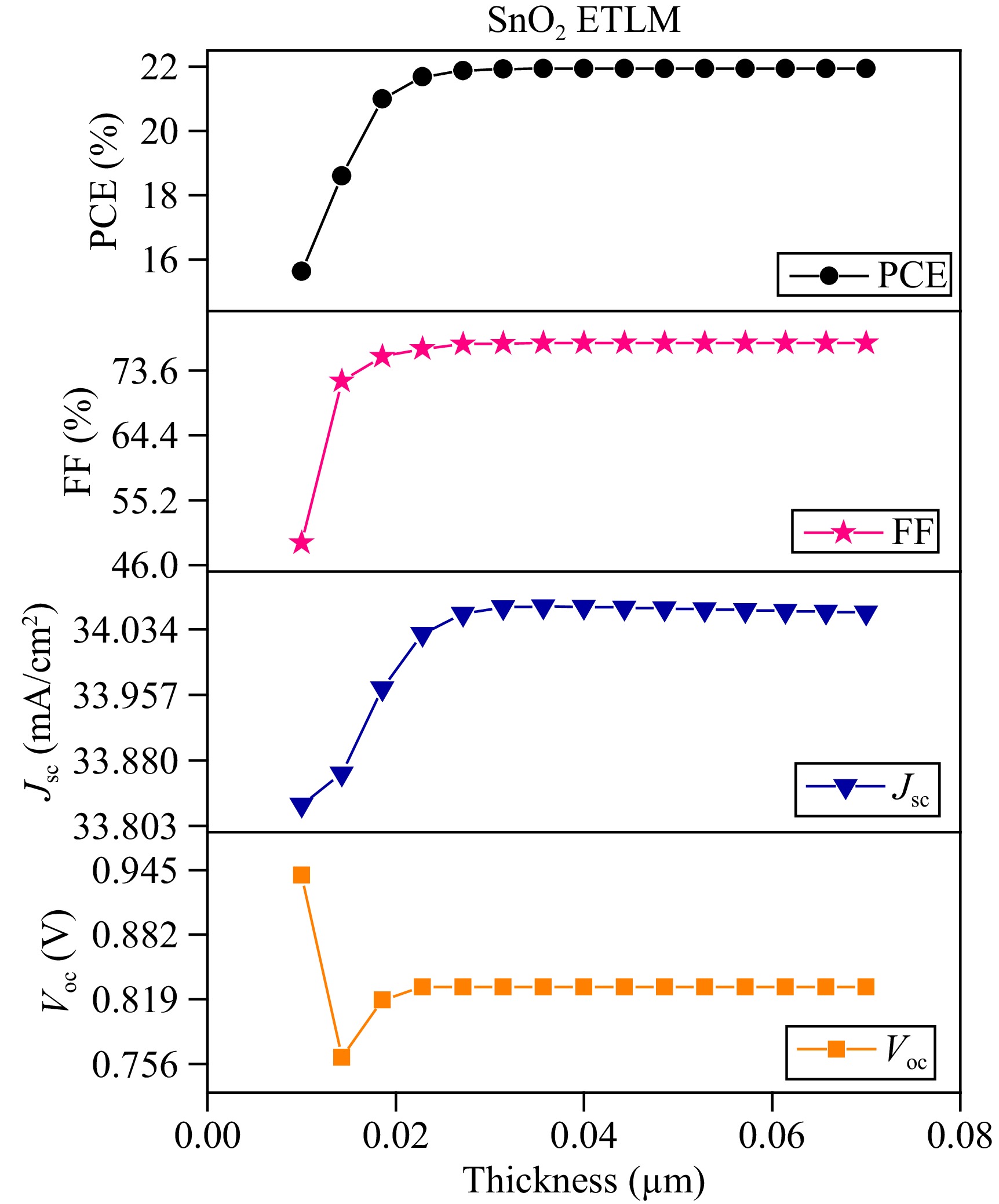
The performance of the proposed device has also been investigated by varying the thickness of the electron transport layer (ETL). As depicted in Fig. 5, the photovoltaic parameters have been examined as a function of ETL thickness, ranging from 0.01 to 0.08 μm. It is noteworthy that all four electrical parameters initially increase with the increasing thickness of the ETL and reach a saturation point at an ETL thickness of 0.044 μm. The PCE of the proposed device increases from 15.6314% at a thickness of 0.01 μm to 21.939% at a thickness of 0.044 μm. The increase in ETL thickness leads to a larger transfer of electrons from the absorber material to the respective electrode, resulting in more charge carriers being transferred to the metal electrode with a thicker ETL. Therefore, after evaluating the simulation results and considering the manufacturing expenditure, an optimized thickness of 0.044 μm is preferably chosen for achieving an optimum solar cell output.
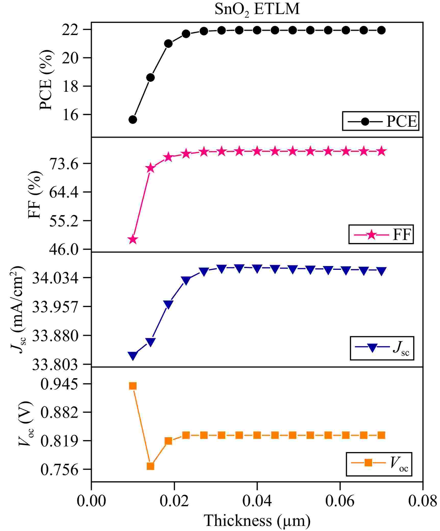
Figure 5.
Impact of ETL thickness variation on solar cell parameters.
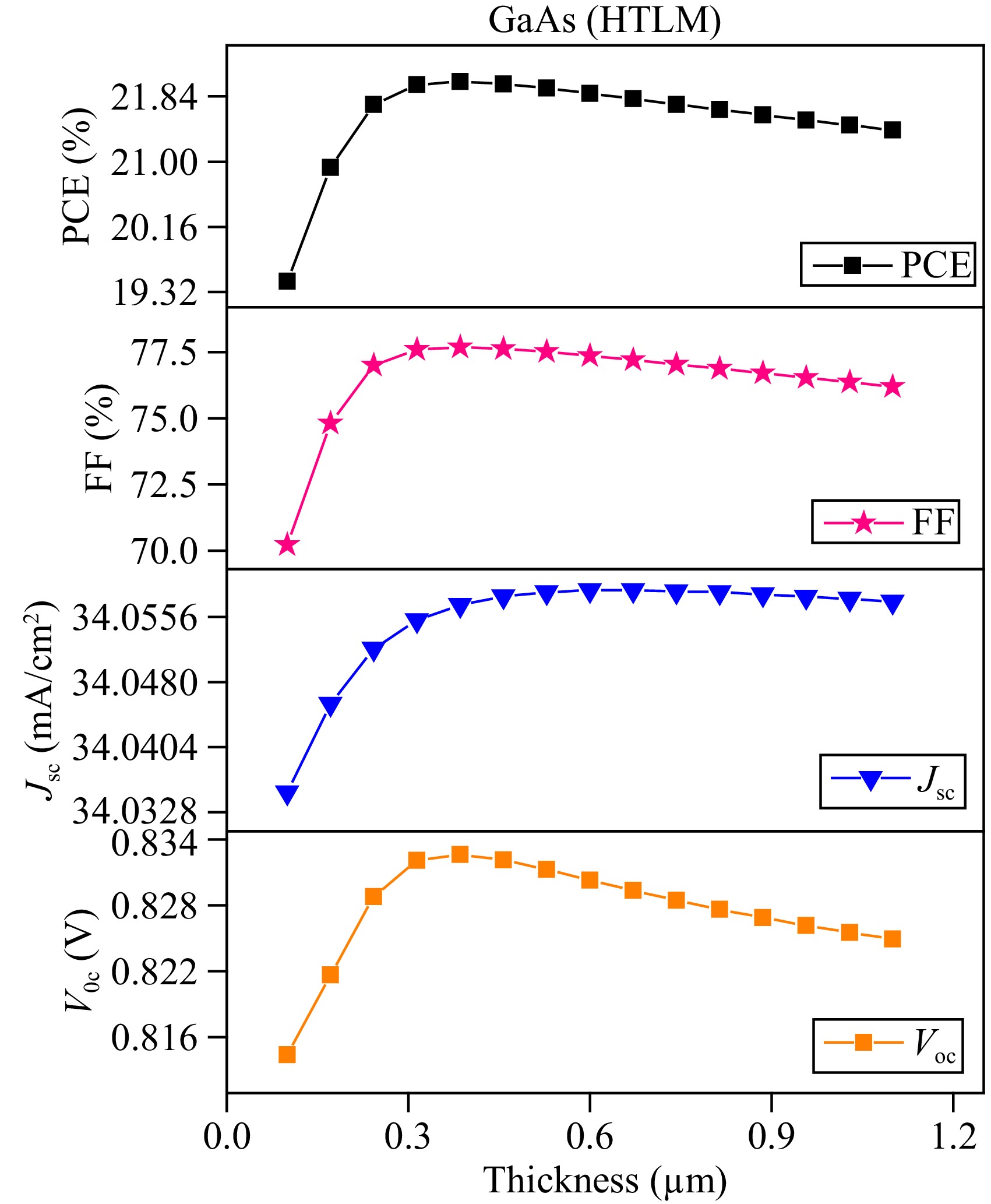
Influence of hole transport layer (HTL) thickness
-
The optimization of the hole transport layer (HTL) thickness is crucial for achieving high efficiency in solar cell devices. Both the electron transport layer (ETL) and HTL play important roles in charge carrier generation and transportation and therefore affect the overall performance of the solar cell. In this study, the thickness of the HTL was varied between 0.1 to 1.1 μm, and the results are presented in Fig. 6. It is observed that the photovoltaic parameters initially increase with increasing HTL thickness up to 0.385 μm, where the maximum efficiency of 22.030% is achieved. Therefore, the optimized thickness of HTL is selected as 0.385 μm. However, as the HTL thickness is increased beyond the optimized value, the solar cell parameters decrease due to an increase in the distance traveled by holes to reach the respective electrode, which results in an increase in the recombination rate. Even if the HTL thickness is too small, it can reduce the uniformity of coverage on the active layer surface.
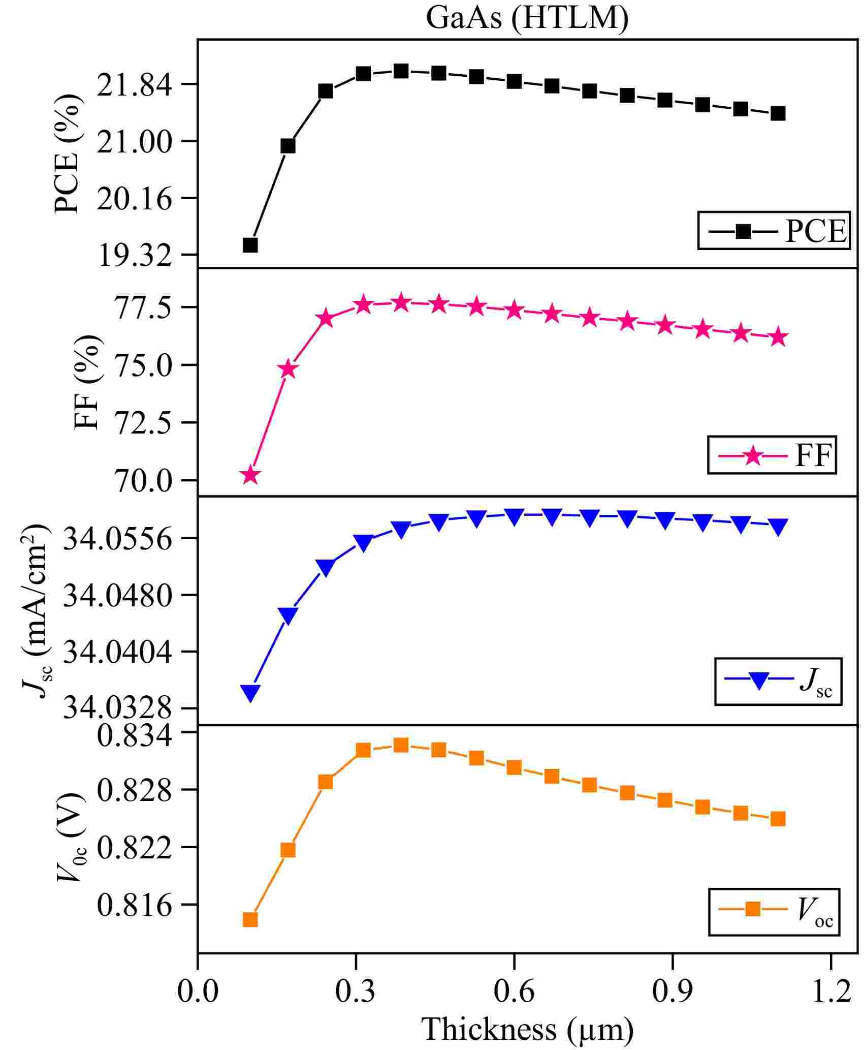
Figure 6.
Impact of HTL thickness variation on solar cell parameters.
Influence of defect density on electrical parameters
-
The optimization of defect density vs electrical parameters is crucial for understanding the operating conditions of the solar cell. The investigation into the defect density at the SnO2/perovskite interface reveals the critical role of interface quality in determining the fill factor and overall efficiency of the solar cell. The optimum value of the defect density have been found to be 1.1 × 1012 cm−2 as shown in Fig. 7. This insight is particularly relevant for the broader field, as it highlights the importance of interface engineering in achieving high-performance solar cells. Researchers working on other types of perovskite or thin-film solar cells may find this information valuable in optimizing their device structures. The optimized parameters obtained from the simulations, including a PCE of 21.93%, fill factor of 77.50%, short-circuit current density (Jsc) of 34.05 mA/cm², and open-circuit voltage (Voc) of 0.83 V, demonstrate the potential of MASnI3-based PSCs to achieve performance metrics comparable to those of lead-based perovskites. The module simulation results, which show an output power of 490.9 watts per panel with 60 cells in series, further emphasize the practical applicability of these findings in real-world solar energy systems.
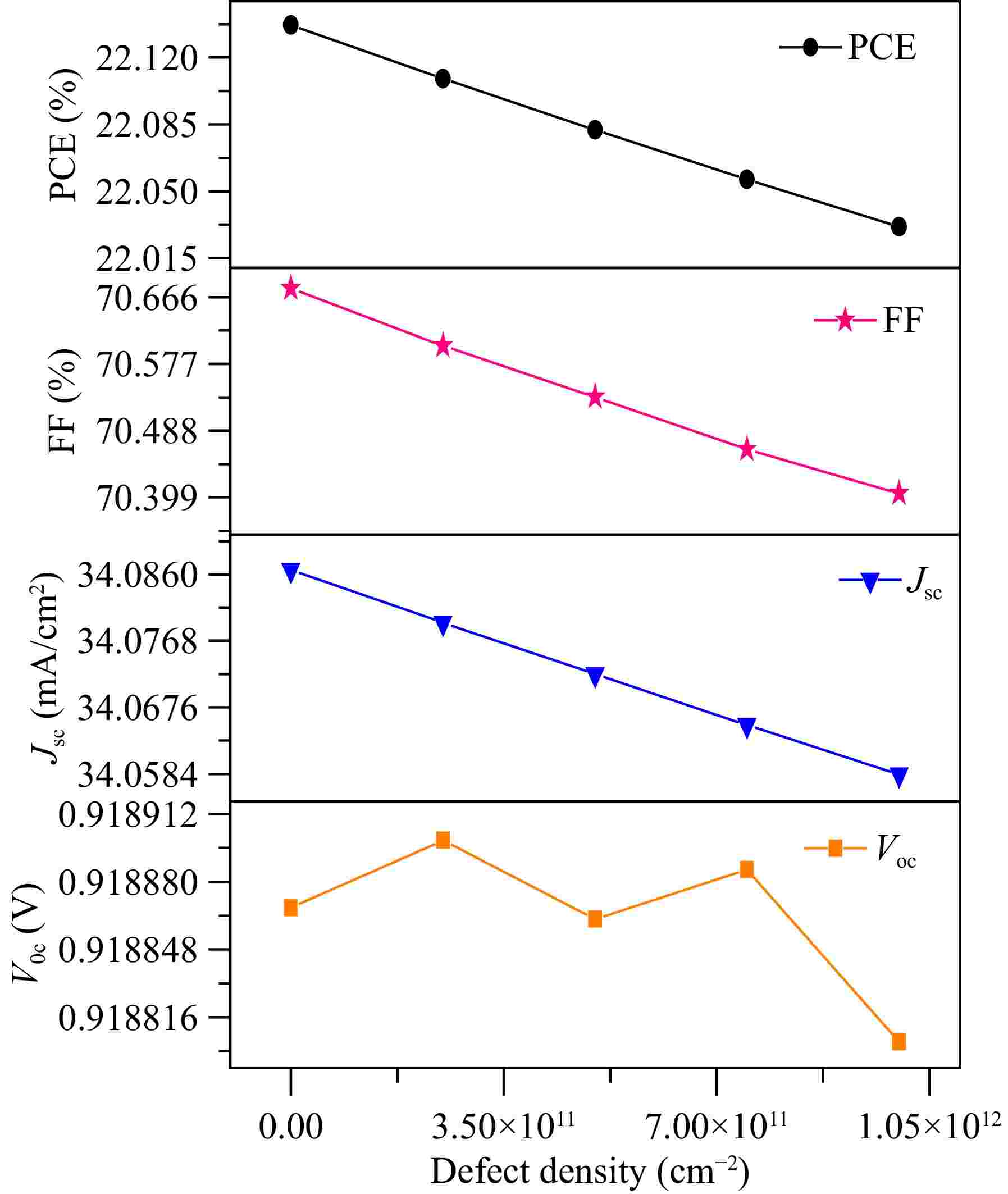
Figure 7.
Defect density versus electrical parameters.
J-V curve of MASnI3-based perovskite solar cell
-
The proposed device's optimized photovoltaic parameters were obtained by analyzing the J-V response of the solar cell, as shown in Fig. 8. The simulation yielded a high PCE of 21.93%, with a high Jsc of 34.05 mA/cm2 and a Voc of 0.83 V. Additionally, the maximum FF value achieved was 77.50%. The results demonstrate that SnO2, an efficient and cost-effective ETL material can replace the comparatively expensive TiO2. Furthermore, GaAs, which possess high hole mobility, can improve the transportation of charge carriers.
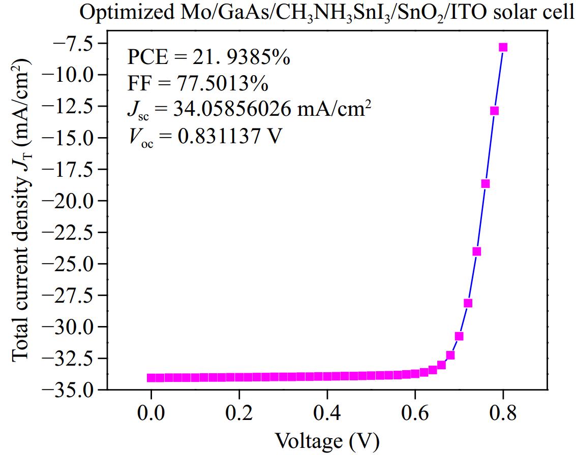
Figure 8.
Graph between current density and voltage.
Optical analysis of proposed perovskite solar cell device
-
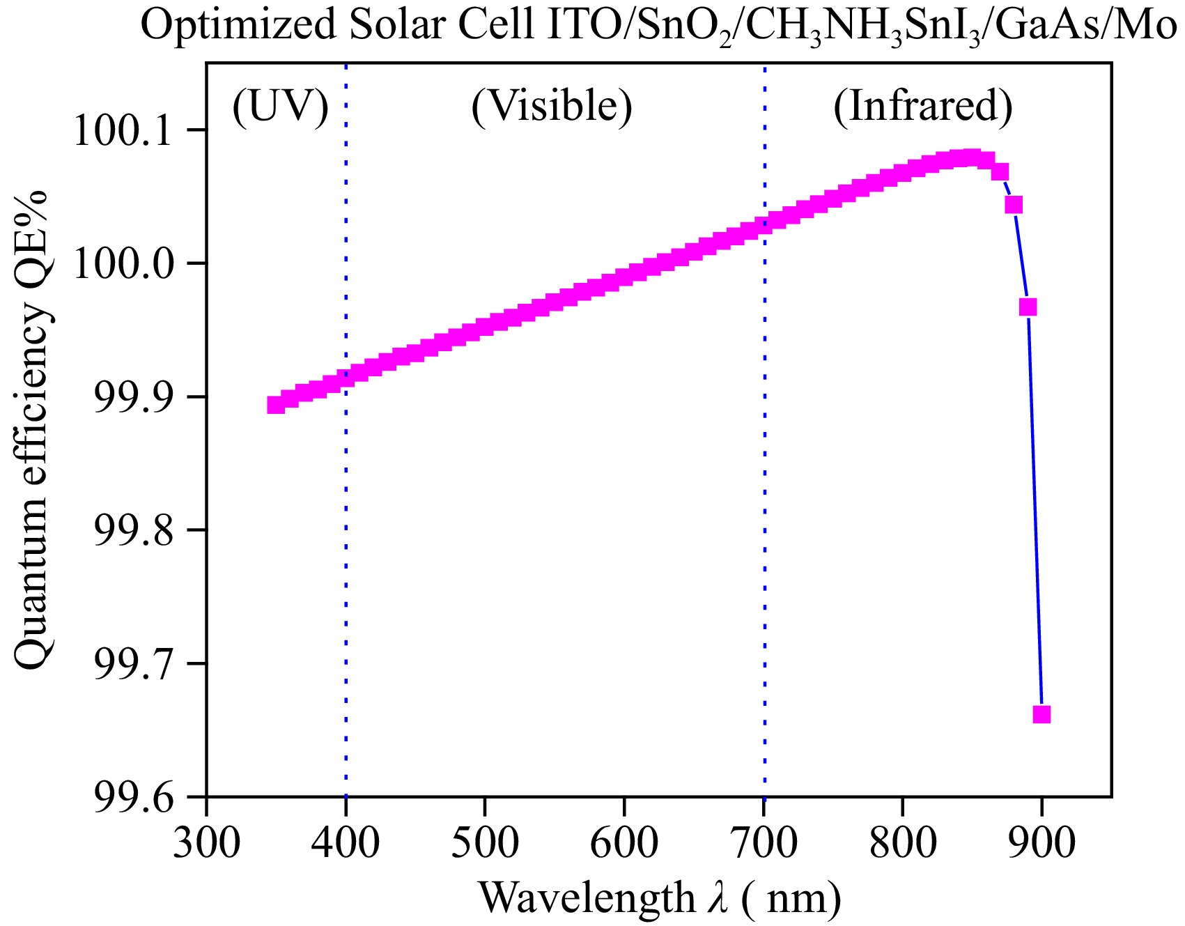
Figure 9 shows the variation in quantum efficiency with different incident wavelengths. Quantum efficiency refers to the ability of a solar cell to generate electron-hole pairs from incident photons of a specific energy. The optical response of the device was analyzed between 350 and 900 nm of wavelength. The results indicate that quantum efficiency increases with an increasing value of wavelength up to 850 nm due to increased optical absorption and photo-generated charge carriers. However, at a wavelength of 900 nm, quantum efficiency drops to 99.66% due to the moderately low band gap of the active layer, which is 1.3 eV. Additionally, Fig. 9 demonstrates that the optimized device structure covers the entire visible region of the spectrum, and its band gap also covers a significant portion of the IR and UV regions.

Figure 9.
Quantum efficiency vs wavelength.
Device variation of interface defect density
-
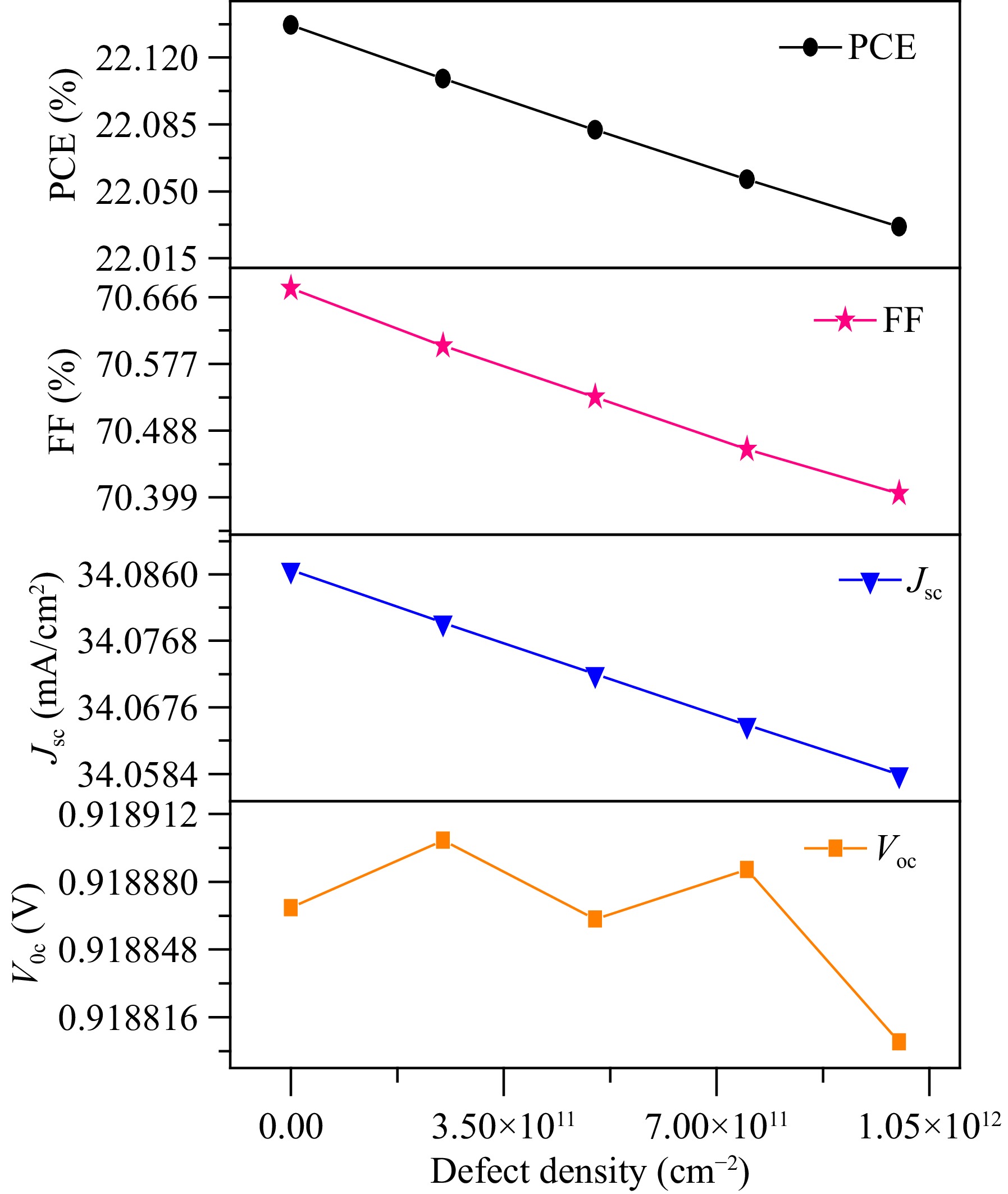
Figure 10 illustrates the impact of SnO2/CH3NH3SnI3 interface defect density on the electrical parameters of the proposed solar cell. Interface defects within the range of 3.29 × 10¹⁷ to 1.316 × 1018 cm−2 were studied. The short-circuit current density, Jsc, shows no noticeable change with variations in interface defect density. However, the open-circuit voltage, Voc, increases from 0.83218 to 3.853V as the value of interface defects increases. The PCE also increases from 22.137% to 26.708% due to the increase in Voc. The fill factor is mainly influenced by the interface defect density, causing it to decrease from 78.0403% to 20.3372% as a result of the parasitic series resistance. Furthermore, all the photovoltaic parameters remain constant after a defect density of 6.58 × 1017 cm−2. Therefore, the optimized value of interface defect density is selected as 6.58 × 1017 cm−2 for optimum device performance.
Figure 10.
Influence of interface defect density on photovoltaic parameters.
Variation in operational temperature
-
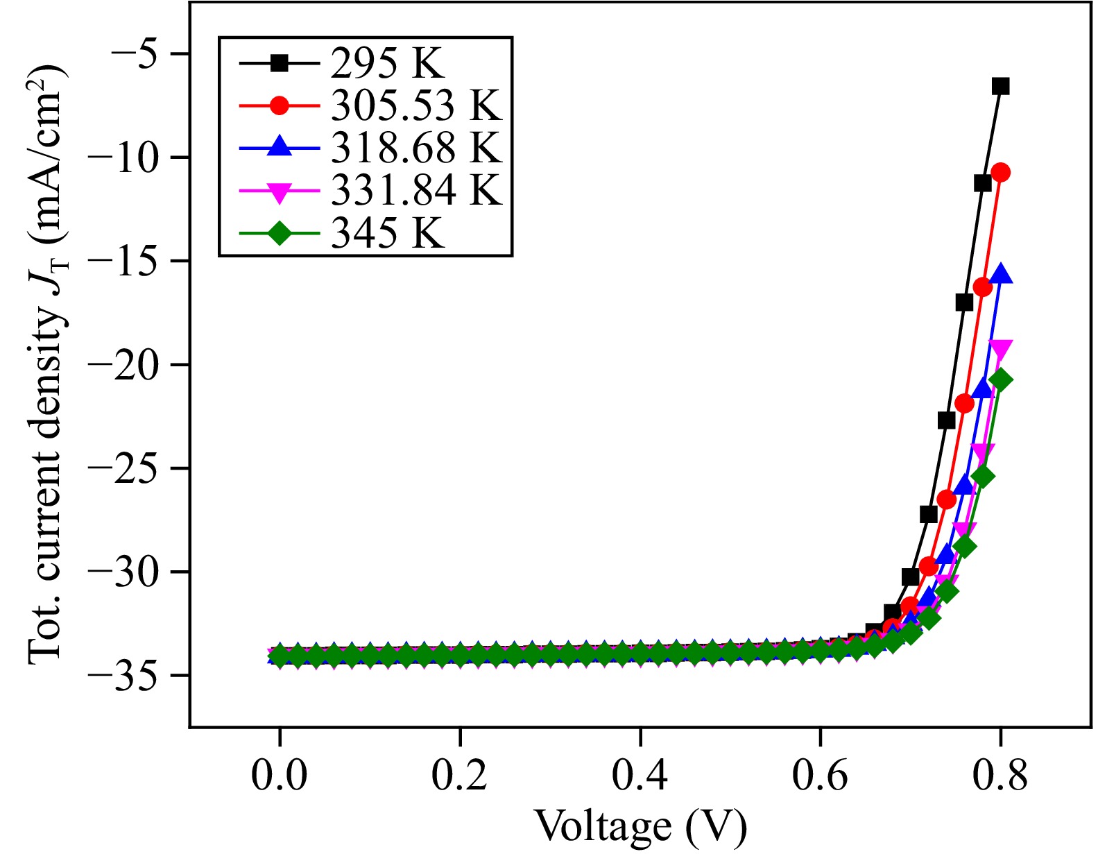
Since the performance of a solar cell greatly depends on the operational temperature, the impact of operating temperature on photovoltaic parameters is also investigated in this study. Figure 11 illustrates the variation in total current density (JT) vs voltage graph in the temperature range of 295 to 345 K. As the temperature increases, stress and deformation occur, leading to an increase in SRH recombination and interfacial defects. Consequently, the diffusion length decreases and series resistance rises. This effect can be verified using the following Eqn (4):
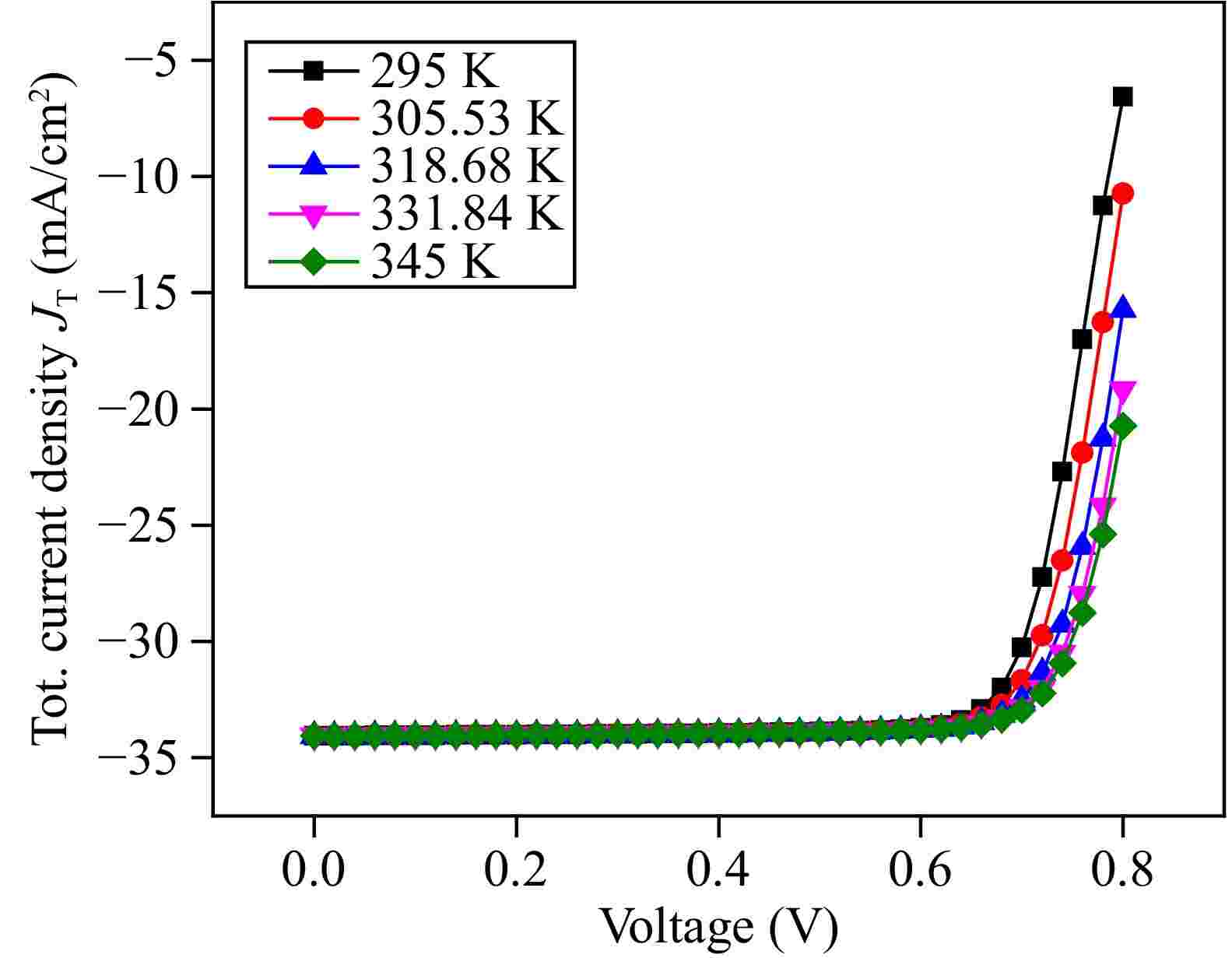
Figure 11.
Influence of temperature on Jsc and Voc.
ddT(Voc)=(Vo−Egq)T (4) where Eg, q, and T are the band gap, electric charge, and temperature of the solar cell respectively. Equation (6) demonstrates that as the operating temperature increases, Voc starts to decrease due to an increase in saturation current and a decrease in PCE[54,55]. Devi et al.[56] also showed that the bandgap, charge carrier mobility, and carrier concentration decrease with an increase in temperature. At a temperature of 295 K, the maximum increase in the value of current density is observed, which is 6.57801 mA/cm2 at a voltage of 0.8 V. Therefore, the optimized value for the operational temperature is 295 K.
Generation-recombination of charge carriers
-
The generation-recombination behavior of charge carriers in relation to the surface depth of the proposed device is depicted in Fig. 12a. The surface depth is studied from the top down to 5.029 μm. At lower surface depth values, the generation rate of charge carriers is low. However, as the surface depth of the solar cell increases, the generation rate shows an upward trend. The generation rate increases rapidly up to 0.385 μm and reaches a maximum value of 1.3695 × 1022 cm−3·s−1 at a depth of 4.985 μm. This is because charge carriers have the maximum diffusion length and mobility within the absorber material of the photovoltaic cell.
A maximum recombination rate of 7.14519 × 1016 cm−3·s−1 has been calculated, which may be attributed to a large number of tin dangling bonds. These dangling bonds cause the absorption of O2 from the air at the SnO2 surface. The absorption of O2 leads to the confinement of electrons in the conduction band of SnO2. As a result, O2 is converted into O−, O2−, and/or O2− ions, which create energy barriers between crystals and increase the recombination rate at the surface of the PSC. This entrapment of charge carriers due to dangling bonds enhances the surface recombination phenomenon, as observed in Fig. 12b. This high surface value can be reduced by minimizing dangling bonds through the use of an appropriate passivation layer at the top of the device or by increasing the doping concentration. The recombination rate decreases as the depth of the solar cell device increases and reaches zero at a depth of 0.385 μm.
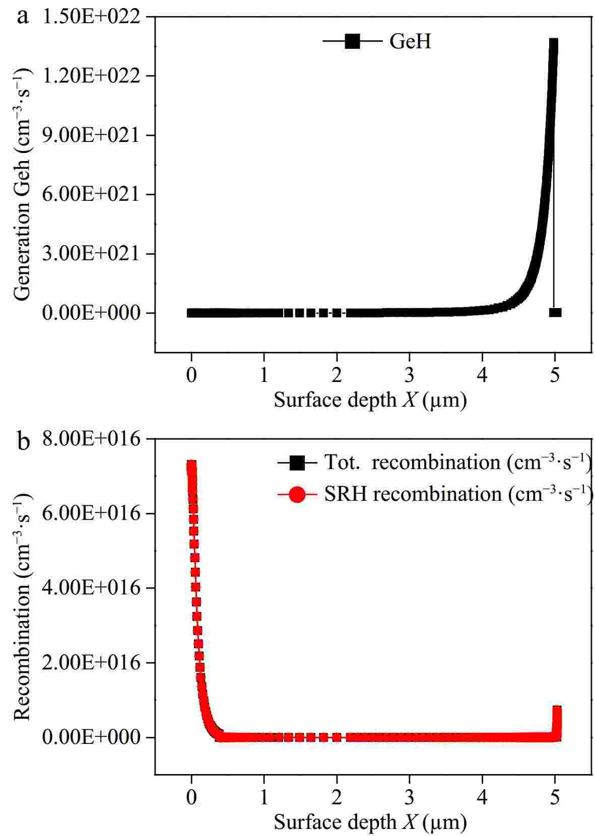
Figure 12.
(a) Variation in generation rate with surface depth of device. (b) Variation in recombination rate with surface depth of device.
Solar module simulations
-
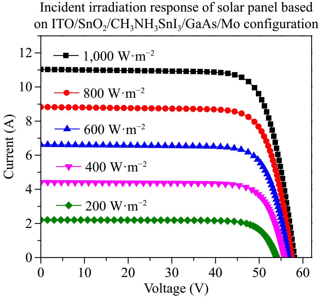
Figure 13 illustrates the incident radiation response of ITO/SnO2/CH3NH3SnI3/GaAs/Mo configuration when used in PVsyst software for simulation of the solar module. The incident radiation intensity was varied from 200 to 1,000 W·m−2 and subsequently the resultant output parameters are plotted. The line graph depicts that current and voltage both are affected by the increase in incident radiation intensity. However, the impact of light intensity on the output current is greater than the output voltage. With the increase in incident light intensity, a considerable increase in output current can be witnessed. It can be seen from the graph, the solar panel current increases linearly with the increase in incident irradiation. The photo-generated current increases from approximately 2 A at a light intensity of 200 W·m−2 to 11 A at a light intensity of 1,000 W·m−2. This is because the increase in incident irradiation intensity, more photons are absorbed by the absorber layer. Consequently, a higher number of photo-generated charge carriers are produced. Hence an increase in the output current is observed. The output voltage also increases gradually with the light intensity. A slight increase in the output voltage from 54 V at 200 W·m−2 to 58 V at 1,000 W·m−2 is observed due to an increased recombination rate at higher voltages.
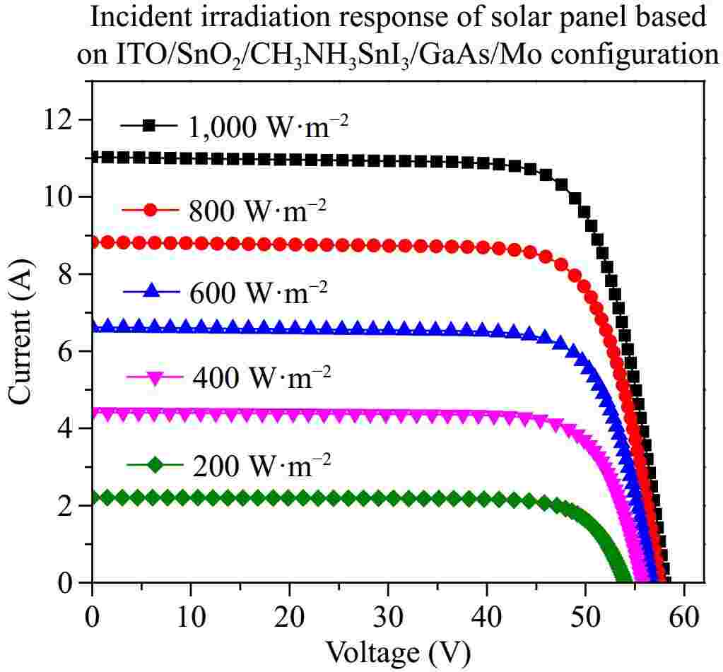
Figure 13.
Impact of light intensity on output characteristics of the solar panel.
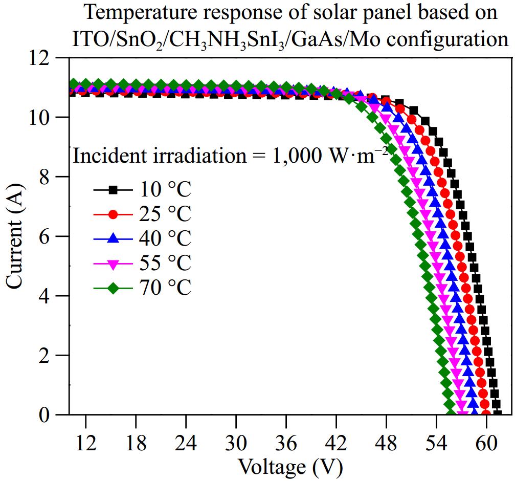
Temperature has a significant effect on the performance of the solar cell. Figure 14 displays the impact of temperature on the solar panel and the corresponding variation in the output parameters. The temperature is varied from 10 to 70 °C at constant light intensity of 1,000 W·m−2. Generally, higher temperature increases the photo-generated current of solar cells because a higher number of charge carriers are produced due to enhanced thermal energy. The increase in the temperature provides additional energy to charge carriers. As a result, the charge carriers overcome the bandgap and more electron-hole pairs are generated. A similar effect can also be observed from the graph shown. According to Fig. 14, the photovoltaic current increases gradually with an increase in temperature i.e., 10.85 A at 10 °C, 10.93 A at 25 °C, 11 A at 40 °C, 11.07 A at 55 °C, and 11.15 A at 70 °C. However, an intersection of individual curves can be observed at voltage 42.5 V. Above 42.5 V the current decreases drastically at higher values of voltage. This is because, beyond a certain point, an increase in voltage accelerates the recombination rate of charge carriers. As a result, the overall current decreases.
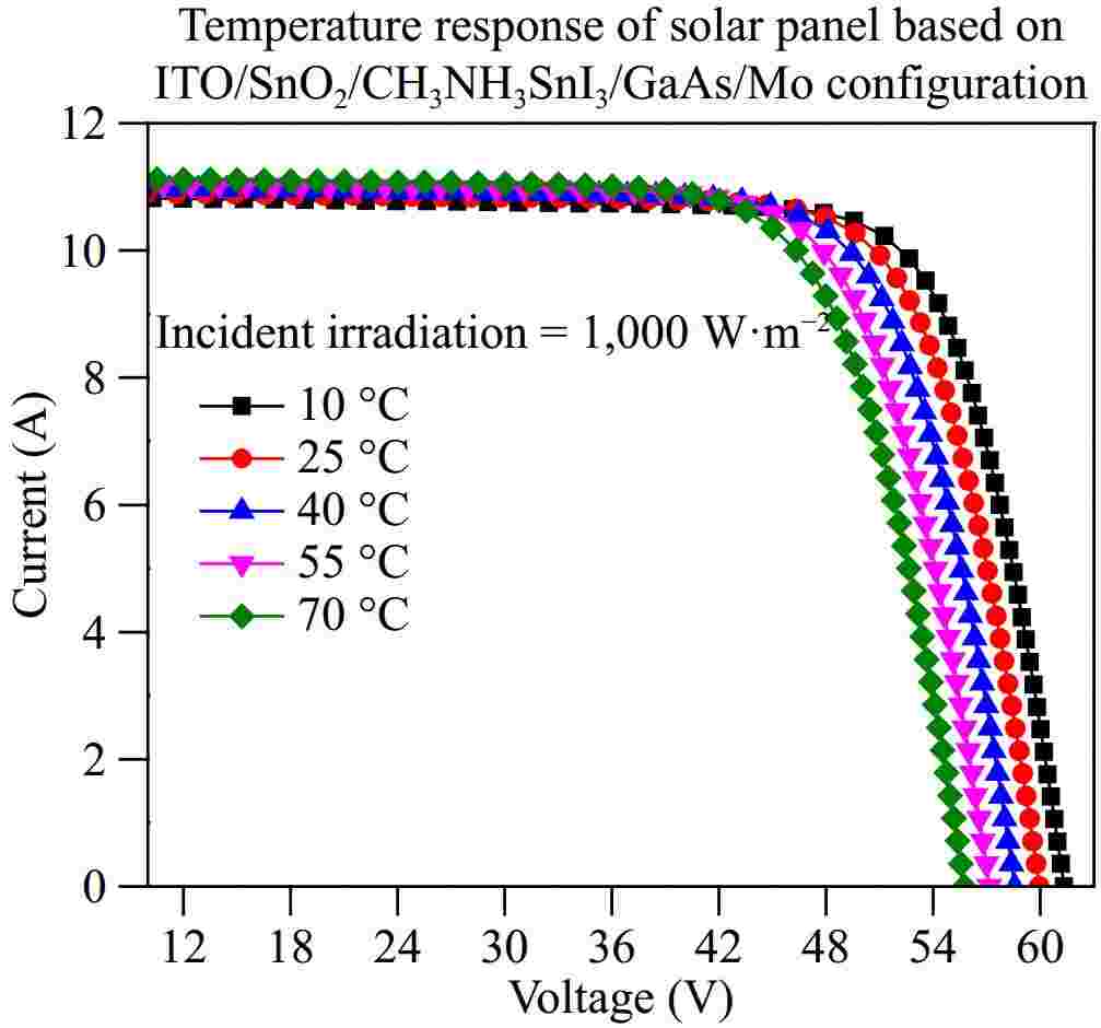
Figure 14.
Effect of temperature on I-V curve of the solar panel.
The effect of incident irradiation on the output power of solar panels is depicted in Fig. 15. The output power shows a linear increasing trend with the increase in incident light intensity. When the incident irradiation intensity is 200 W·m−2, the maximum output power is 94.6 W. As the light intensity is increased to 1,000 W·m−2, the maximum output power also increases to 490.9 W. The incident irradiation intensity determines the number of photons interacting with the absorber layer of the photovoltaic cell per unit time. At higher intensities, a greater number of electron-hole pairs are generated within the material which leads to an increased value of output power. Hence the power generation ability of the solar cell can be tuned by adjusting the incident light intensity. The overall output is decreased if the charge carriers transport mechanism is not sufficient enough to overcome the recombination rate.
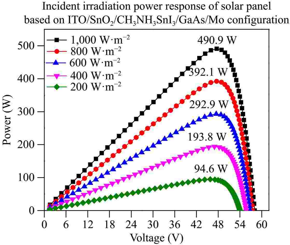
Figure 15.
Influence of light intensity on the output power of the solar panel.
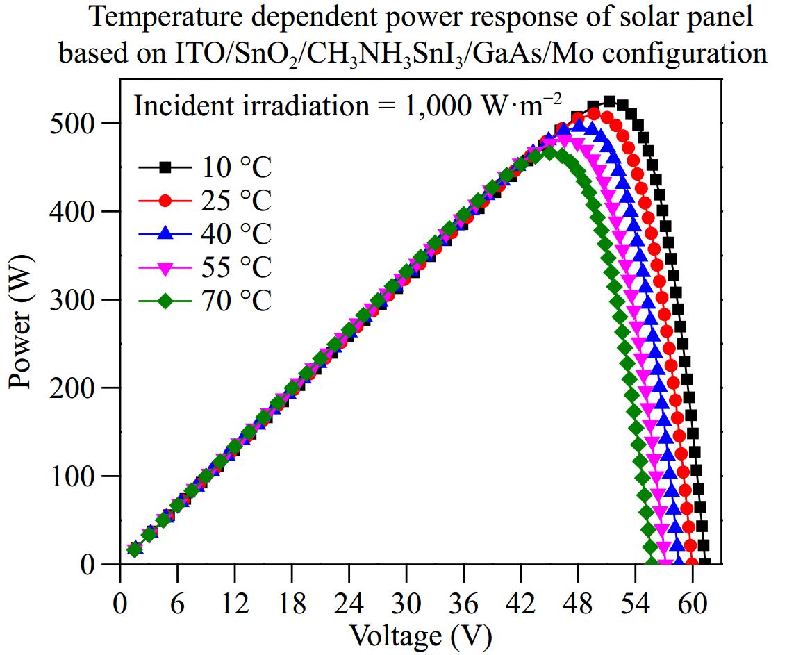
The line graph in Fig. 16 illustrates the effect of temperature on the power generation performance of the solar panel. The operating temperature of the solar panel is varied from 10 to 70 °C at constant irradiation intensity of 1,000 W·m−2. The increase in temperature of the solar cell has a negative impact on the output power. The maximum output power shows a linear downward trend with the rise in temperature. From Fig. 16, it is inferred that output power is closely related to the operational temperature of the solar cell. The maximum output at 10 and 70 °C is recorded as 524.3 and 466.1 W respectively. Hence increase in temperature increases the series resistance resulting in reduced current flow and sequentially leading to decreased efficiency and output power.

Figure 16.
Dependance of output power on the temperature of the solar panel.
The explorations of this study have several important implications for the broader field of solar energy research, particularly in the ongoing development of lead-free PSCs. The exploration of tin-based perovskites, such as methyl ammonium tin iodide (MASnI3), represents a significant advancement in the search for environmentally friendly and stable alternatives to the widely used lead-based perovskites. This research contributes that MASnI3-based solar cells, when paired with efficient electron and hole transport layers, can achieve performance metrics that are competitive with their lead-based counterparts. One of the key contributions of this study is the identification of SnO2 as a superior electron transport layer (ETL) for MASnI3-based PSCs. The improved stability and efficiency achieved by using SnO2 instead of the traditional TiO2 address a critical challenge in the field: the long-term operational stability of tin-based PSCs. This insight could guide future research in optimizing ETL materials, not only for tin-based perovskites but also for other emerging photovoltaic materials that require enhanced stability. Additionally, the use of GaAs as a hole transport layer (HTL) compatible with the MASnI3 absorber layer has been shown to improve the overall device performance. By systematically varying the thickness of functional layers and analyzing the impact on photovoltaic parameters, our study provides valuable guidelines for optimizing the design of tin-based PSCs. These findings could influence the broader field by encouraging researchers to explore alternative HTL and ETL materials that may further improve the performance and stability of perovskite solar cells.
-
Methyl ammonium tin iodide (MASnI3) solar cells demonstrate comparable device performance to lead-based perovskite solar cells. This study aims to enhance the device stability and electro-optical properties of tin-based perovskite solar cell devices. The simulation of an MASnI3-based solar cell with an efficient SnO2 electron transport layer (ETL) was conducted using SCAPS software (Version 3.3.08). SnO2 is a proficient ETL material that can replace TiO2 to address stability concerns in the solar cell. The SnO2-based ETL has increased the output efficiency of tin halide PSC in this work. Additionally, GaAs is a competent hole transport layer (HTL) material that is compatible with the MASnI3 absorber layer. Simulation results indicate that increasing the thickness of the absorber and ETL layers enhances the characteristic parameters of the photovoltaic cell. Conversely, in the case of the HTL, these electrical parameters decrease with increasing thickness of the HTL material. The optimized values for the HTL, ETL, and absorber functional layers are 0.385 μm, 0.044 μm, and 4.6 μm, respectively. Furthermore, an analysis is performed at the SnO2/perovskite interface by varying the defect density, revealing that defect density primarily affects the fill factor of the solar cell. The optimal value for the interface defect density is selected as 6.58 × 1017 cm−2, resulting in an efficiency of 26.70%. The spectral response of our optimized structure demonstrates maximum photon absorption within the visible region of the spectrum. The rise in device temperature decreases carrier mobility, which in turn reduces the PCE of the device. Therefore, 295 K is selected as the optimized value for the operating temperature. After simulations, the optimized parameters of the proposed device are a PCE of 21.93%, FF of 77.50%, Jsc of 34.05 mA·cm−2, and Voc of 0.83 V. It is concluded that the beneficial results obtained from this research study provide valuable information for further investigation of tin-based PSC with the aim of improving efficiency, increasing device stability, and making the photovoltaic parameters comparable to those of the lead-based counterpart. Use of input parameters of a single cell in module simulation package has resulted in a healthy output power of 490.9 watts per panel consisting of 60 cells in series. The presented investigation may prove to be a step forward toward exploration of novel solar cells and their modules to address the global energy generation issues. In the broader context of solar energy research, this study represents a step forward in the development of sustainable and high-performance solar cell technologies. By addressing key challenges such as device stability, material compatibility, and interface quality. It also contributes to the ongoing effort to make solar energy more efficient, reliable, and environmentally friendly. The insights gained from this study could inspire further exploration of novel materials and device architectures, ultimately advancing the field toward the goal of widespread adoption of solar energy as a clean and sustainable energy source.
-
The authors confirm contribution to the paper as follows: writing, investigation: Basit A; conceptualization, writing, project administration, software, supervision: Qasim I. Both authors reviewed the results and approved the final version of the manuscript.
-
The data utilized in this article has not been previously submitted in any repository. To ensure transparency and facilitate further research, the data may be made available for academic and research purposes by emailing the corresponding author.
-
The authors wish to extend their sincere gratitude to Dr. Marc Burgelman and his esteemed team at the Electronics and Information Systems (ELIS) Laboratory, University of Ghent, Belgium, Dr. A. Mermoud and M. Villoz at Geneva University, Switzerland, for granting access to the simulation software.
-
The authors declare that they have no conflict of interest.
- Copyright: © 2025 by the author(s). Published by Maximum Academic Press, Fayetteville, GA. This article is an open access article distributed under Creative Commons Attribution License (CC BY 4.0), visit https://creativecommons.org/licenses/by/4.0/.
-
About this article
Cite this article
Basit A, Qasim I. 2025. Optimizing solar cell and module design with SnO2-ETL and organometal-halide perovskite absorber: SCAPS-1D and PVSyst analysis. Wireless Power Transfer 12: e001 doi: 10.48130/wpt-0024-0015 

Figure 1.
Schematic structure of proposed device ITO/SnO2/CH3NH3SnI3/GaAs/Mo.