


-
Wireless power transfer (WPT) technology effectively addresses convenience and safety issues associated with conductive charging, drawing significant attention from both industry and academia[1]. Within the domain of WPT applied to electric vehicle (EV) charging, inductive power transfer (IPT) technology has emerged as the preferred solution for wireless EV charging due to its high power and efficiency capabilities[2,3]. Multiple countries and organizations have released standards concerning static wireless power transfer (SWPT) for EVs[4,5], commencing a new phase for SWPT production, testing, and commercialization. However, the widespread adoption of EVs is hampered not only by charging concerns. Range anxiety, along with the cost and size of battery packs, remains a key challenge for the EV industry. Consequently, researchers have proposed dynamic wireless power transfer, building upon SWPT. By enabling contactless charging of in-motion vehicles, DWPT technology offers the potential for EVs to carry reduced or even no battery packs, while simultaneously extending driving range and further enhancing the convenience and safety of energy supply.
Consequently, the magnetic coupler remains a critical electromagnetic conversion component, with coupler design exerting a more prominent impact on charging than SWPT due to dynamic driving constraints. To mitigate coupling fluctuation effects during driving, research on DWPT magnetic couplers primarily focuses on two categories: long track-type and array-type couplers. The long track-type magnetic coupler's core principle is coil extension; specifically, elongating transmitting (Tx) coils along the driving direction achieves a stable magnetic field over longer distances, suppressing coupling fluctuations. Long track-type couplers are further classified by track polarity into unipolar and bipolar: unipolar tracks feature elongated, travel-direction-staggered coils, while bipolar tracks interleave magnetic poles between coils using wave or layered winding configurations[6]. The Korea Advanced Institute of Science and Technology (KAIST) has extensively researched both types, releasing six generations of On-line Electric Vehicles (OLEV) since 2009[7,8], some tested and operated on public roads. A meander type Tx coil[9], comprising multiple serpentine-wound elongated conductors; when energized with multiphase power, phase differences in the excitation source produces a traveling magnetic field aligned with vehicle motion. IKERLAN enhanced this design in 2017[10], but the Tx coil's relatively large width resulted in a suboptimal transmission distance-to-width ratio.
The array-type magnetic coupler employs discrete Tx coils arranged in an array, each structurally resembling coils in SWPT systems. Achieving dynamic charging necessitates continuous switching of multiple Tx coils, demanding precise position detection and switching control. Furthermore, magnetic field variations between adjacent coils induce coupling fluctuations, thus leading to output power fluctuations. Consequently, mitigation of output power fluctuations constitutes a critical research priority for array-type couplers. Owing to the structural simplicity of individual coils, diverse configurations exist globally, including UoA's DD coil arrays[11−13], Michigan State University's multi-coil arrays[14], ORNL's CP coil arrays[15], Fukuoka University's three-phase coil arrays[16], and Chongqing University's embedded coil arrays[17], and interleaved DD coil arrays[18].
Research on mitigating power fluctuations in arrayed magnetic couplers has progressed significantly. To stabilize the coupling coefficient, an alternately arranged segmented transmitter track using rectangular-solenoid pads was proposed to achieve magnetic field complementation[19]. Similarly, an integrated magnetic coupler where compensation inductors are embedded into main coils was utilized to suppress fluctuations within ± 4% without adding external components[20]. Beyond structural modifications, active control strategies have also been explored. An array-type segmented structure that activates multiple rows of transmitting coils was introduced, utilizing a secondary-side Buck-Boost converter to suppress fluctuations in real-time[21]. Furthermore, a self-adaptive two-pole receiver was developed to ensure interoperability and output stability across different transmitter polarities[22]. While effective, these methods often necessitate specialized hardware or complex sensing systems. Consequently, further refinement is required in establishing systematic analytical models that can optimize universal and widely used coil forms.
The design of the compensation network is as critical as that of the magnetic coupler for DWPT systems. Owing to advantages such as a reduced number of active components, simpler control, and higher efficiency, DISO systems have garnered more research interest than MISO systems[23]. Various compensation strategies have been explored to mitigate output power fluctuations. These include LCC networks on the transmitter side to maintain a constant current[24], a hybrid LCL-LC topology that leverages distinct responses to mutual inductance for smoother power transfer[25,26], and an optimized T-type network to minimize the power fluctuation factor under varying coil spacing. Similarly, an LCL-S compensated DISO system demonstrated that output power and efficiency are positively correlated with the sum of the Tx-Rx coupling coefficients under constant input and load conditions[27]. While these methods improve power stability by addressing specific issues like current variations, they commonly neglect the impact of cross-coupling between Tx coils on the input characteristics. This omission can destabilize the input impedance, leading to practical challenges such as the loss of ZVS and increased reactive power losses.
In summary, current research on array-type magnetic couplers faces two primary limitations. Structurally, while coil optimization and DISO architectures can mitigate mutual inductance fluctuations, the design process remains largely empirical, lacking a systematic theoretical foundation. This frequently leads to complex coupler structures, which increase manufacturing costs and fabrication difficulty. In terms of circuit topology improvement, research on DISO systems has predominantly focused on LCL-type compensation networks, while neglecting the adverse effects of cross-coupling. This neglect inevitably leads to impedance mismatch under dynamic operating conditions, degrading power transfer stability.
To overcome these limitations, this paper presents a dynamic wireless power transfer system utilizing a DISO architecture, combined with a CLC compensation network. By establishing a comprehensive theoretical model that accounts for cross-coupling, a systematic parameter tuning strategy and an optimized coupler design methodology are developed. The proposed solution effectively suppresses output power fluctuations without complex structural modifications to the coupler. Moreover, it compensates for the impedance mismatch caused by cross-coupling, ensuring stable power transfer under dynamic conditions.
-
The proposed system utilizes a secondary-side, single-element CLC-S compensation network to minimize the weight and complexity of EV WPT systems. This network provides constant-voltage output under varying loads and exhibits increasing input impedance as the Rx moves away from the Tx. These characteristics significantly simplify position detection and power-switching control, allowing a Tx coil to be energized before the vehicle enters and de-energized after it departs, as illustrated in Fig. 1. Consequently, a smooth output power profile is maintained as the Rx coil gradually disengages from one Tx coil while concurrently drawing power from the adjacent one.
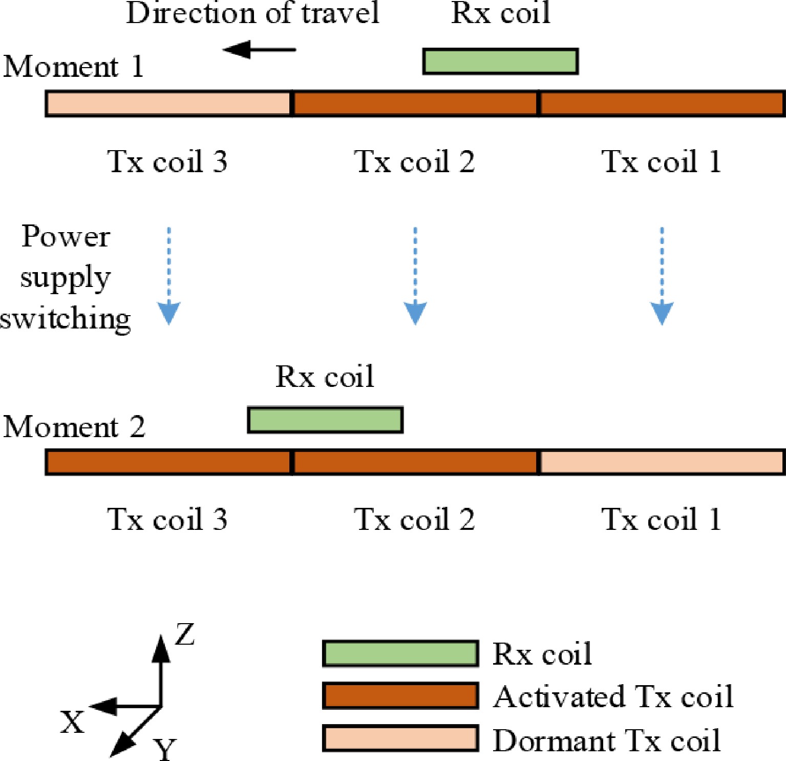
Figure 1.
Power supply timing model for an array-type DWPT system.
Array-type magnetic coupler circuit model
-
The typical mutual inductance model for array-type systems is represented by the structure shown in Fig. 1.
In Fig. 2, M01, M02, ..., M0n denote the mutual inductances between receiver coils 1 to n, and receiver coil 0, where n represents the maximum number of participating receiver coils for power transfer. Similarly, M12, M13, ..., M1n, ..., M(n−1)n represent the mutual inductances between transmitter coils on the same side. V denotes the complex voltage at coil terminals, and I denotes the complex current within coils, with subscripts corresponding to coil numbering. The complex inductance relationships depicted in Fig. 2 can be concisely expressed in matrix form as follows:
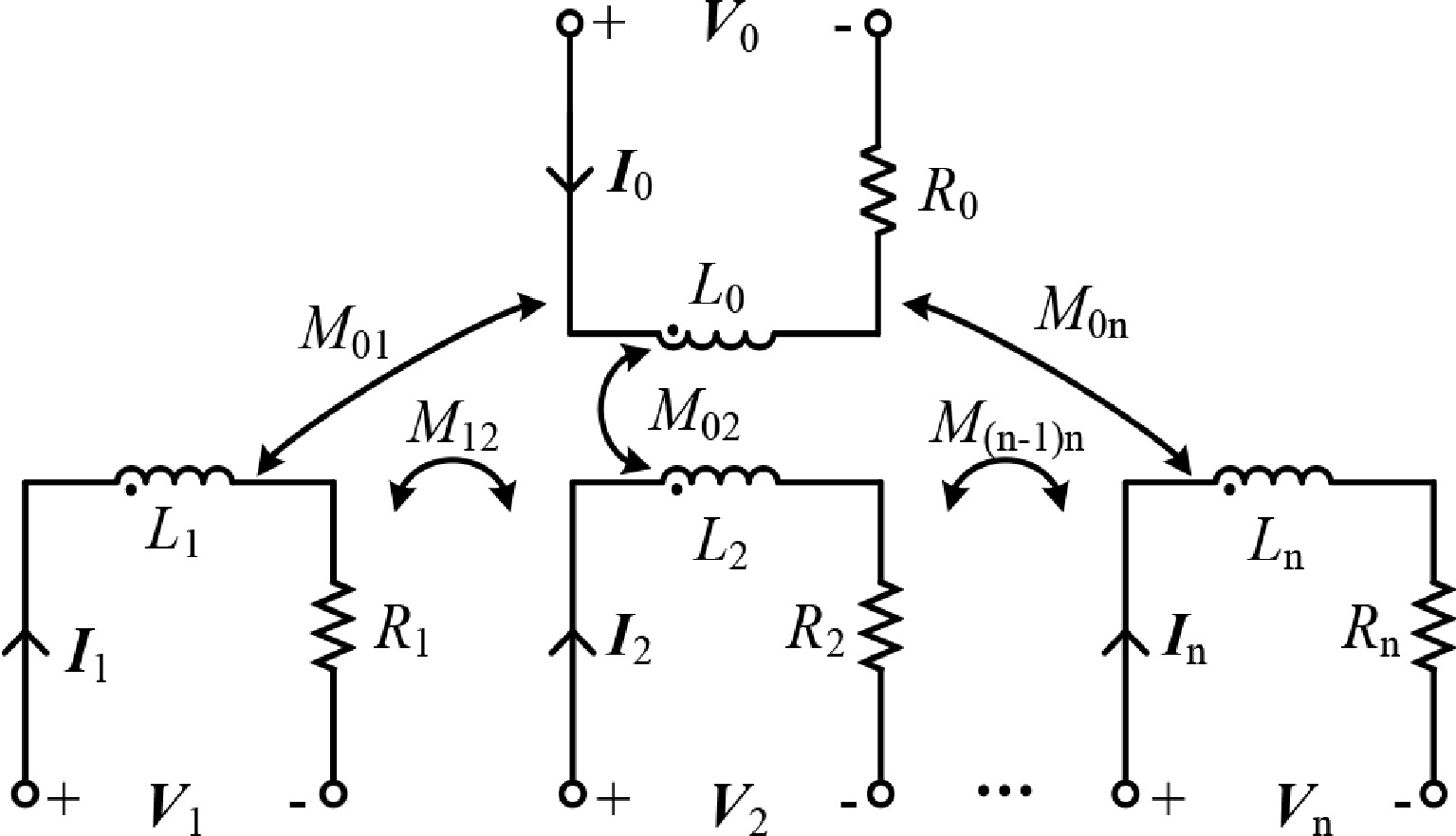
Figure 2.
Typical mutual inductance model of an array-type DWPT system.
$ \mathbf{L}=\left[\begin{matrix} {L}_{0} & -{M}_{01} & -{M}_{02} & \cdots\\ {M}_{10} & {L}_{1} & -{M}_{12} & \cdots\\ {M}_{20} & -{M}_{21} & {L}_{2} & \cdots\\ \cdots & \cdots & \cdots & \cdots\\ {M}_{\text{n}0} & -{M}_{\text{n1}} & \cdots & -{M}_{\text{n}(\text{n}-1)} \end{matrix} \left.\begin{array}{c} -{M}_{\text{0n}}\\ -{M}_{1\text{n}}\\ \cdots\\ -{M}_{(\text{n}-1)\text{n}}\\ {L}_{\text{n}} \end{array}\right]\right. $ (1) To represent interactions between Rx and Tx coils, as well as among individual Rx coils, the circuit is modeled using controlled voltage sources. Based on this approach, the controlled-source model for the array-type DWPT system is further illustrated in Fig. 3.
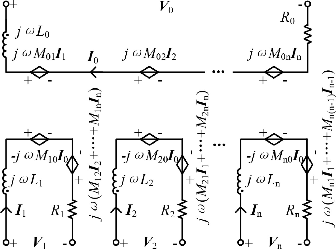
Figure 3.
Controlled source model of an array-type DWPT system.
Characteristics of the CLC-S compensated DISO system
-
In the DISO system, only two Tx coils operate simultaneously. Consequently, the equivalent circuit of the CLC-S compensated DISO WPT system is depicted in Fig. 4.
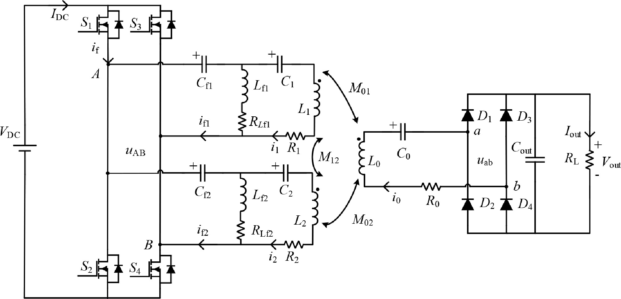
Figure 4.
CLC-S compensated DISO system.
In Fig. 4, VDC is the DC voltage output from the primary PFC to two high-frequency inverters; IDC represents the DC currents; uAB represents the corresponding inverter output voltages; uAB is the input voltage of the Rx rectifier bridge; Lf1, Cf1, C1, Lf2, Cf2, and C2 are the compensating inductance and capacitance for Tx coils 1 and 2, respectively; L1, L2, and L0 represent the self-inductance of Tx coils 1 and 2, and the Rx coil; R1, R2, R0, RLf1, and RLf2 represent the internal resistance of corresponding inductors. The DC load RL and its current and voltage are Iout and Vout, respectively.
Based on the model in Fig. 4, the following equations are derived using KVL:
$ \left\{\begin{aligned} & {U}_{\text{AB}}={I}_{\text{f1}}\cdot \left(\dfrac{1}{j\omega {C}_{\text{f1}}}+j\omega {L}_{\text{f1}}\right)-\dfrac{{I}_{1}}{j\omega {C}_{\text{f1}}}\\ &{I}_{\text{f1}}\cdot j\omega {L}_{\text{f1}}={I}_{1}\cdot \left(j\omega {L}_{\text{f1}}+j\omega {L}_{1}+\dfrac{1}{j\omega {C}_{1}}\right)-j\omega {M}_{01}{I}_{0}+j\omega {M}_{12}{I}_{2}\\ &{U}_{\text{AB}}={I}_{\text{f2}}\cdot \left(\dfrac{1}{j\omega {C}_{\text{f2}}}+j\omega {L}_{\text{f2}}\right)-\dfrac{{I}_{2}}{j\omega {C}_{\text{f2}}}\\ &{I}_{\text{f2}}\cdot j\omega {L}_{\text{f2}}={I}_{2}\cdot \left(j\omega {L}_{\text{f2}}+j\omega {L}_{2}+\dfrac{1}{j\omega {C}_{2}}\right)-j\omega {M}_{02}{I}_{0}+j\omega {M}_{12}{I}_{1}\\ &0={I}_{0}\cdot \left(\dfrac{1}{j\omega {C}_{0}}+j\omega {L}_{0}+R\right)-j\omega {M}_{01}{I}_{1}-j\omega {M}_{02}{I}_{2} \end{aligned} \right.$ (2) Under resonance conditions, the following relationships are satisfied for the compensation components:
$ \begin{split}\omega &=\dfrac{1}{\sqrt{{L}_{\text{f1}}{C}_{\text{f1}}}}=\dfrac{1}{\sqrt{\left({L}_{1}+{L}_{\text{f1}}\right){C}_{1}}}=\dfrac{1}{\sqrt{{L}_{\text{f2}}{C}_{\text{f2}}}}\\ &=\dfrac{1}{\sqrt{\left({L}_{2}+{L}_{\text{f2}}\right){C}_{2}}}=\dfrac{1}{\sqrt{{L}_{0}{C}_{0}}} \end{split} $ (3) The resonant cavity current satisfies:
$ {i}_{1}=j\omega {u}_{1}{C}_{\text{f1}},\;\;{i}_{2}=j\omega {u}_{1}{C}_{\text{f2}} $ (4) Applying the First-Harmonic Approximation (FHA), the full-bridge rectifier is approximated as a resistive load. Consequently, the rectifier's input voltage (u1), and output voltage (u0) are derived as follows:
$ \left\{\begin{aligned} &{u}_{1}=\dfrac{4}{\pi }{V}_{\text{dc}}\sin (wt)\\ &{u}_{0}={i}_{0}{R}_{\text{eq}}={i}_{0}\dfrac{8}{{\pi }^{2}}{R}_{\text{L}} \end{aligned}\right. $ (5) To ensure consistent rail output performance, and simplify the analysis, circuit parameter deviations between transmission channels are neglected. Given uAB = u1, Cf1 = Cf2 = Cft, L1 = L2 = Lt, C1 = C2 = Ct, R1 = R2 = Rt, the simplified system is shown in Fig. 5. Applying these equivalence conditions:
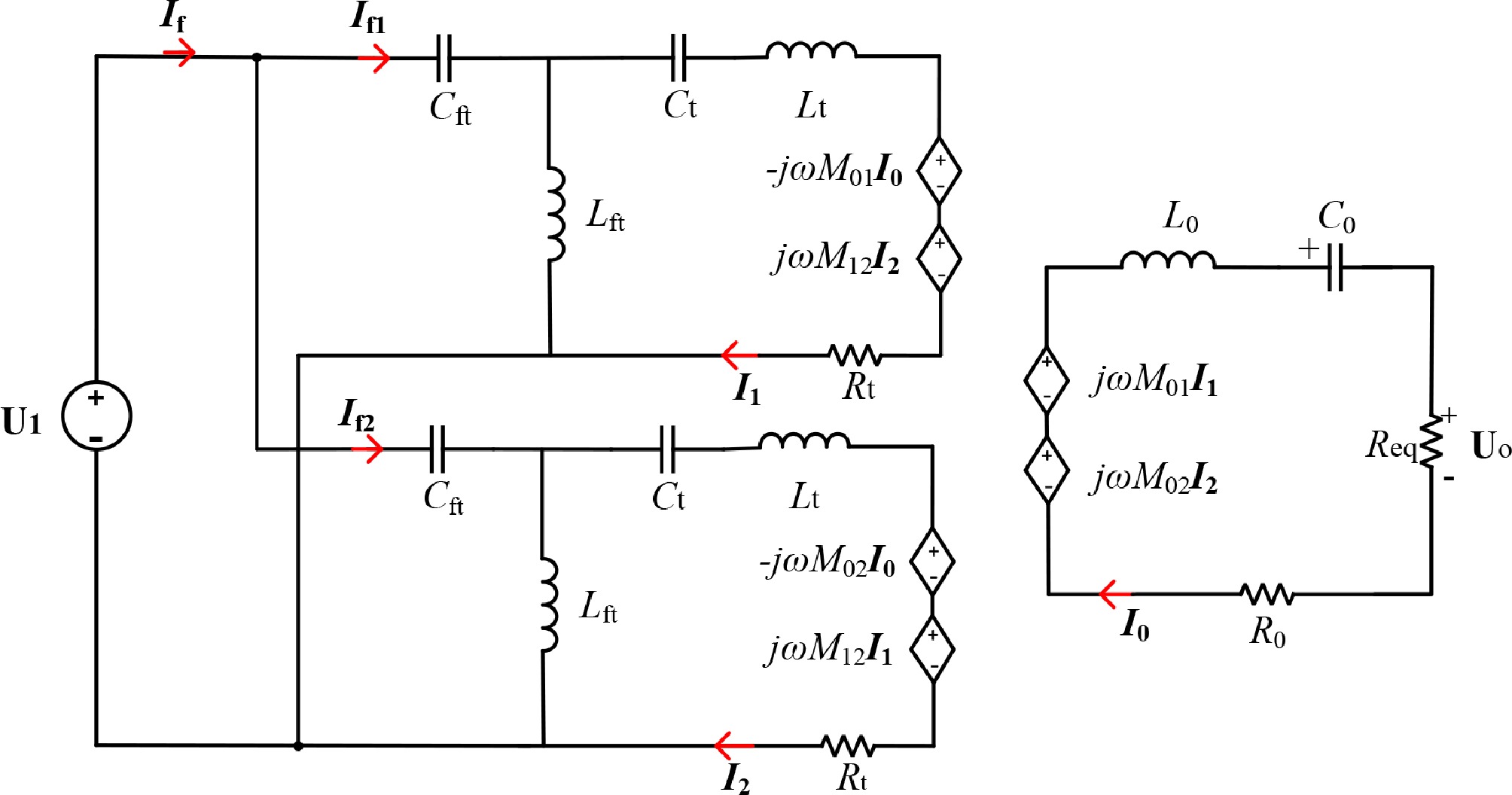
Figure 5.
Simplified equivalent circuit of a CLC-S compensated DISO system.
$ \left\{\begin{aligned} &{I}_{\text{f1}}=\dfrac{C_{\text{ft}}^{\text{2}}{U}_{1}{\omega }^{4}M_{\text{01}}^{\text{2}}}{{R}_{\text{eq}}}+\dfrac{C_{\text{ft}}^{2}{U}_{1}{\omega }^{4}{M}_{01}{M}_{02}}{{R}_{\text{eq}}}+jC_{\text{ft}}^{\text{2}}{U}_{1}{\omega }^{3}{M}_{12}\\ &{I}_{\text{f2}}=\dfrac{C_{\text{ft}}^{\text{2}}{U}_{1}{\omega }^{4}{M}_{01}{M}_{02}}{{R}_{\text{eq}}}+\dfrac{C_{\text{ft}}^{\text{2}}{U}_{1}{\omega }^{4}M_{02}^{2}}{{R}_{\text{eq}}}+jC_{\text{ft}}^{\text{2}}{U}_{1}{\omega }^{3}{M}_{12}\\ &{I}_{\text{f}}={I}_{\text{f1}}+{I}_{\text{f2}}=\dfrac{{U}_{1}{({{M}_{01}}+{{M}_{02}})}^{2}{\omega }^{4}C_{\text{ft}}^{\text{2}}}{{R}_{\text{eq}}}+2jC_{\text{ft}}^{2}{U}_{1}{\omega }^{3}{M}_{12}\\ &{I}_{0}=-\dfrac{{C}_{\text{ft}}{U}_{1}{\omega }^{2}({M}_{01}+{M}_{02})}{{R}_{\text{eq}}} \end{aligned} \right.$ (6) As expressed in Eq. (6), If denotes the inverter output, current, while I0 corresponds to the system output current. Equation (6) demonstrates that system output current stabilizes when the sum of mutual inductances between the dual Tx coils and Rx coil remains constant. The coil overlapping design constraining the mutual inductance variation will be detailed in in a further section. Under this condition, the phase of the inverter output currents depends solely on the cross mutual inductance M12 between the primary Tx coils. To eliminate M12's adverse effects, compensation topology parameters must be specifically designed for M12.
For CLC-S compensation topologies, the increased number of components offers greater control flexibility, where tuning compensation parameters significantly enhances system performance. To identify optimal control parameters, sensitivity analysis of compensation topology parameters must be conducted. Given that capacitor adjustments (via capacitor arrays or PWM modulation) are more feasible than inductor modifications, this study focuses specifically on analyzing how variations in the three key capacitor parameters affect circuit characteristics. Consequently, the system's input impedance Zin (considering C0, C1 and C2) is given as follows:
$ Z\text{in}=\dfrac{-j}{\omega C_{\text{f1}}}+(j\omega L_{\text{f}1}\parallel D) $ (7) Where
$ \begin{split} & D=Z_1+Z_{\mathrm{ref}} \\ &Z_\text{ref}=\dfrac{(\omega M)^2}{Z_2} \\ &Z_{\text{1}}=j\omega L_{\text{1}}-\dfrac{j}{\omega C_{\text{1}}} \\ &Z_{\text{2}}=R_{\mathrm{eq}}+j\omega L_{\text{2}}-\dfrac{j}{\omega C_{\text{0}}} \end{split} $ (8) As shown in Fig. 6a, b, the effects of ± 20% capacitor parameter variations on output power and input impedance angle are demonstrated. The impact on output power is evaluated using the ratio Po/Po_ ref, where Po denotes output power at deviated capacitance values, and Po_ ref represents output power at ideal resonant capacitance. Analysis reveals:
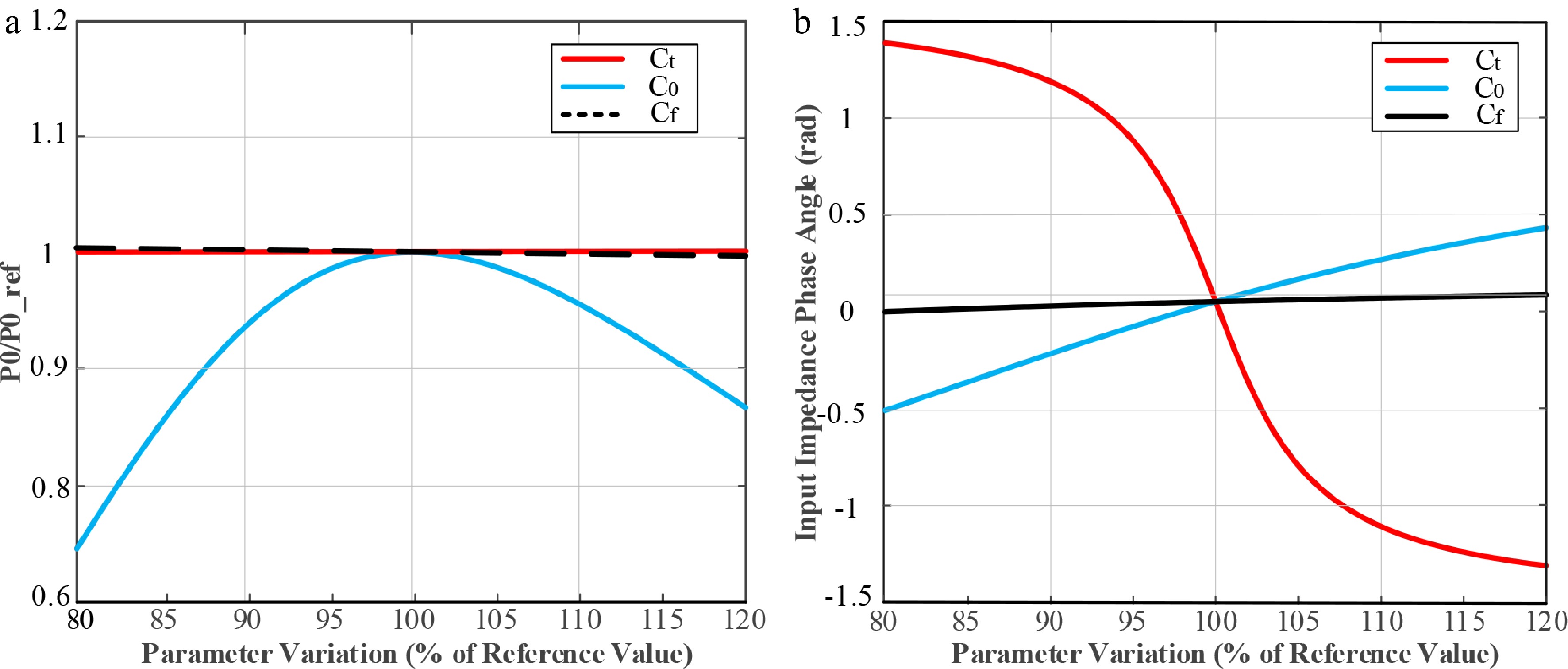
Figure 6.
The transfer characteristics vs compensation capacitance: (a) output power; (b)input impedance phase angle.
● Output power exhibits low sensitivity to series compensation capacitors Ct and Cf.
● Output power is highly sensitive to secondary-side series capacitor C0.
Given the system's design objective of power stability, only Ct and Cf are considered. Figure 6b further shows that the input impedance angle is minimally affected by Cf, precluding its use for compensating cross-coupling effects (M12).
Comprehensively, tuning
$ {{C}}_{\mathrm{t}} $ $ \left\{\begin{aligned} & {I}_{\text{0}}=-\dfrac{{C}_{\text{ft}}{U}_{1}{\omega }^{2}({M}_{01}+{M}_{02})}{{R}_{\text{eq}}}\\ &{I}_{\text{f}}=\dfrac{{({{M}_{01}}+{{M}_{02}})}^{2}{\omega }^{4}C_{\text{ft}}^{\text{2}}{U}_{1}}{{R}_{\text{eq}}}+j\cdot 2{C}_{\text{ft}}\omega {U}_{\text{1}}\left({C}_{\text{ft}}{\omega }^{2}({L}_{1}+{M}_{12})+1-\dfrac{{C}_{\text{ft}}}{{C}_{\text{t}}}\right) \end{aligned} \right.$ (9) From Eq. (7), it can be observed that the output current I0 is independent of Ct. Thus, the system output power is expressed as:
$ {P}_{\text{out}}=I_{0}^{2}R=\dfrac{{\omega }^{4}u_{1}^{2}C_{\text{ft}}^{\text{2}}{\left({M}_{\text{01}}+{M}_{\text{02}}\right)}^{2}}{{R}_{\text{eq}}} $ (10) Proceeding to derive the relationship between the system impedance angle and Ct:
$ \theta =\arctan \left(\dfrac{2{R}_{\text{eq}}\left({C}_{\text{t}}\left[1+({L}_{\text{t}}+{M}_{12}){\omega }^{2}{C}_{\text{ft}}\right]-{C}_{\text{ft}}\right)}{{({{M}_{01}}+{{M}_{02}})}^{2}{\omega }^{3}{C}_{\text{t}}{C}_{\text{ft}}}\right) $ (11) As derived from Eq. (9), adjusting Ct enables regulation of the system impedance angle while maintaining output power stability.
Compared to wired charging, the structure and communication processes of WPT systems for electric vehicles are more complex, requiring compliance with electromagnetic interference (EMI) standards during engineering implementation. EMI research in WPT systems primarily focuses on ZVS in power converters to significantly suppress EMI. To realize ZVS for MOSFETs, the body diode must conduct before the MOSFET conducts. Taking switch S1 in Fig. 4 as an example, the MOSFET must be turned on under negative current. Owing to current symmetry characteristics, satisfying the condition IZVS = 2CossVDC/td in Eq. (10) ensures ZVS for all switches, where IZVS is the ZVS current threshold, Coss the MOSFET output capacitance, td the dead time, and If_off the current at turn-on instant.
$ -{I}_{\text{ZVS}}\geq {I}_{\text{f}\_\text{off}} $ (12) Considering minor fluctuations in the main mutual inductance sum and cross-coupling, a 10% design margin is typically retained to account for these variations:
$ -{I}_{\text{ZVS}}\geq 90\text{% }{I}_{\text{f}\_\text{off}} $ (13) The preceding analysis employs the FHA, neglecting higher-order harmonics. However, these harmonics influence instantaneous current values, thereby affecting the charge dissipation rate from capacitors during dead time, which impacts ZVS implementation. Consequently, harmonic current components must be considered in current calculations. For higher-order CLC-type compensation networks, the inductor-capacitor network from primary to secondary sides acts as a high-order filter. At higher harmonic frequencies, interactions between primary and secondary sides become negligible[28]. Thus, higher-order harmonics in the inverter output current can be preliminarily estimated as:
$ \begin{split} &{\mathbf{I}}_{\text{f}\_\text{3rd}}\approx -\dfrac{{\mathbf{U}}_{\text{1}\_\text{3rd}}}{j\cdot 3{\omega }_{\text{0}}{L}_{\text{ft}}+\dfrac{1}{j\cdot 3{\omega }_{\text{0}}{C}_{\text{ft}}}}=j\dfrac{3{\mathbf{U}}_{\text{1}\_\text{3rd}}}{8{\omega }_{0}{L}_{\text{ft}}}\\ &{\mathbf{I}}_{\text{f}\_\text{5th}}\approx -\dfrac{{\mathbf{U}}_{\text{1}\_\text{5th}}}{j\cdot 5{\omega }_{\text{0}}{L}_{\text{ft}}+\dfrac{1}{j\cdot 5{\omega }_{0}{C}_{\text{ft}}}}=j\dfrac{5{\mathbf{U}}_{\text{1}\_\text{5th}}}{24{\omega }_{0}{L}_{\text{ft}}}\\ &\qquad\qquad\qquad\qquad\cdots\\ &{\mathbf{I}}_{\text{f}\_\text{(2k+1)th}}\approx -\dfrac{{\mathbf{U}}_{\text{1}\_\text{(2k+1)th}}}{j\cdot (2\mathrm{k}+1){\omega }_{0}{L}_{\text{ft}}+\dfrac{1}{j\cdot (2k+1){\omega }_{0}{C}_{\text{ft}}}}\\ &\qquad\;\;\quad=j\dfrac{(2k+1){\mathbf{U}}_{{1_(2{\mathrm{k}}+1){\mathrm{th}}}}}{\left({(2k+1)}^{2}-1\right){\omega }_{\text{0}}{L}_{\text{ft}}}\\ &\qquad\qquad\qquad\qquad\cdots \end{split} $ (14) According to Eq. (12), the phase difference between
$ {\mathbf{U}}_{1\_ \text{mth}} $ $ {\mathbf{I}}_{\mathrm{f}\_ \text{mth}} $ $ {\mathbf{U}}_{1} $ $ \begin{split}\max \left\{\sum{i}_{\text{f}\_\text{m}\,\text{th}}\right\}&=\sqrt{2}\cdot \sum\limits_{k=1}^{\mathrm{\infty }}{I}_{\text{f}\_\text{(2k+1)}\,\text{th}}\\ &=\sqrt{2}\cdot \sum\limits_{k=1}^{\mathrm{\infty }}\dfrac{1}{{(2k+1)}^{2}-1}\dfrac{{U}_{1}}{\omega {L}_{\text{ft}}}=\dfrac{\sqrt{2}}{4}\cdot \dfrac{{U}_{1}}{\omega {L}_{\text{ft}}} \end{split} $ (15) According to Eq. (13), the harmonic-induced current at switch turn-on remains constant under constant input voltage. For the DISO system employed here, harmonic currents in the parallel dual-input channels exhibit identical magnitude and phase, consequently superposing additively at the inverter port. Thus, the current If_off at switch turn-on is given by:
$ {I}_{\text{f}\_\text{off}}=2{C}_{\text{f}1}\omega {U}_{1}\left({C}_{\text{ft}}{\omega }^{2}({L}_{1}+{M}_{12})+1-\dfrac{{C}_{\text{ft}}}{{C}_{1}}\right)-\dfrac{\sqrt{2}}{2}\cdot \dfrac{{U}_{1}}{\omega {L}_{\text{ft}}} $ (16) Combining with Eq.(16), the expression for Ct satisfying the ZVS condition is derived as:
$ {C}_{\text{t}}\leq \dfrac{{C}_{\text{f}}}{\dfrac{10}{9}{I}_{\text{ZVS}}+{C}_{\text{ft}}{\omega }^{2}({L}_{1}+{M}_{12})+1-\dfrac{\sqrt{2}}{4}} $ (17) Through the analysis, adjusting Ct achieves ZVS. However, it must be noted that excessive Ct tuning causes significant phase deviation between If and u1, increasing reactive power. This elevates inductor branch currents and reduces system efficiency. Therefore, when harmonic current superposition in dual channels satisfies ZVS requirements, the optimal Ct adjustment targets zero imaginary component in If, achieving minimized reactive power.
$ {u}_{\text{1}}-\dfrac{{u}_{1}{C}_{\text{ft}}}{{C}_{\text{t}}}+{\omega }^{2}{u}_{1}{C}_{\text{ft}}{L}_{\text{t}}+{\omega }^{2}{M}_{12}{u}_{1}{C}_{\text{ft}}\text=0 $ (18) Based on Eq.(18), the mathematical relationship between the resonant capacitance Ct and cross-coupling effects (M12) under this requirement is derived.
$ {C}_{\text{t}}=\dfrac{1}{{\omega }^{2}\left({M}_{12}+{L}_{\text{t}}+{L}_{\text{ft}}\right)} $ (19) Based on the preceding analysis, the parameter design methodology for achieving ZVS during dynamic operation in CLC-S compensated DISO wireless charging systems has been established. Subsequently, coil design optimization will be implemented to suppress fluctuations in the sum of mutual inductances.
Mutual inductance of the DISO magnetic coupler
-
Through the analysis in previous section, it can be seen that the sum of M01 and M02 directly affects the stability of the output of the CLC-S DISO system. Therefore, to moderate the fluctuation of the output power, the magnetic couplers need to be designed to mitigate the variation of M01 + M02.
Impact of the misalignment between the Tx and Rx coils
-
To clarify the variation of the mutual inductance of the magnetic coupler with the movement of the vehicle, firstly, pre-fetch the parameters of the Tx coils of the magnetic coupler according to Table 1, with the relevant variable definitions in the table as shown in Fig. 7.
Table 1. Pre-fetched parameters of the Tx coil.
Symbol Value Symbol Value t1 2 mm FEL 150 mm t2 12 mm FEW 150 mm t3 2 mm ALL 200 mm t4 12 mm ALW 200 mm aL> 100 mm μ0 4π × 10−7 N/A2 aW 100 mm μ1 (μ4) 1.000021 hgap 90 mm μ2 (μ3) 2,300 z1 1.5 mm σ0 0 S/m z2 61.5 mm σ1 (σ4) 3.8 × 10⁷ S/m z3 63 mm σ2 (σ3) 0.1538 S/m n1 15 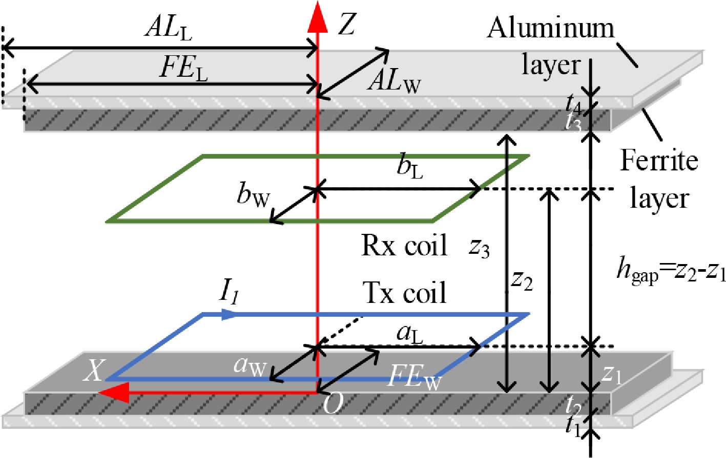
Figure 7.
Schematic diagram of the magnetic coupler.
Assuming that the dimensions and turns of the Rx coil are the same as those of the Tx coil. The fluctuation of the mutual inductance of the magnetic coupler with the misalignment between the Rx coil and the Tx coil is simulated using the example of a single square coil.
The point P(0, 0, z3) is defined as the center of the coil plane of the Rx coil. In this example, the variation of the mutual inductance of the magnetic coupler when x changes and y = 0 can be obtained through simulation analysis, as shown in Fig. 8.
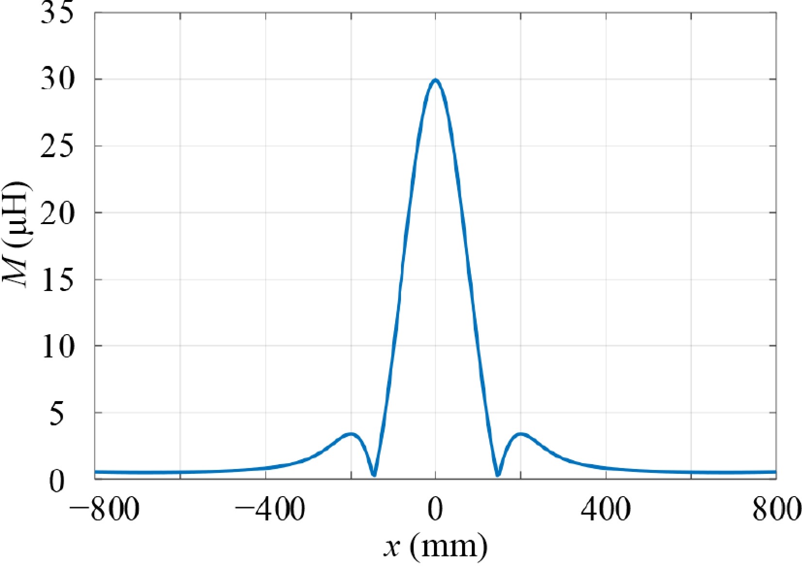
Figure 8.
Characteristic curve of M as a function of the position of the Rx coil.
It can be observed that using the pre-selected magnetic coupler parameter combination in Table 1, the width of the region with low mutual inductance change rate is very narrow. It can be calculated that only 66.44% of the area can achieve a mutual inductance value exceeding half of the maximum mutual inductance value.
By appropriately extending the length of the Tx coil in the X direction, a more uniform magnetic field distribution can be obtained during the offset process. When the length of the Tx coil is extended from 100 to 250 and 400 mm, the change curve of mutual inductance M is shown in Fig. 9. Extending the coil length helps achieve stable power transmission in the system, but may lead to electromagnetic leakage issues.
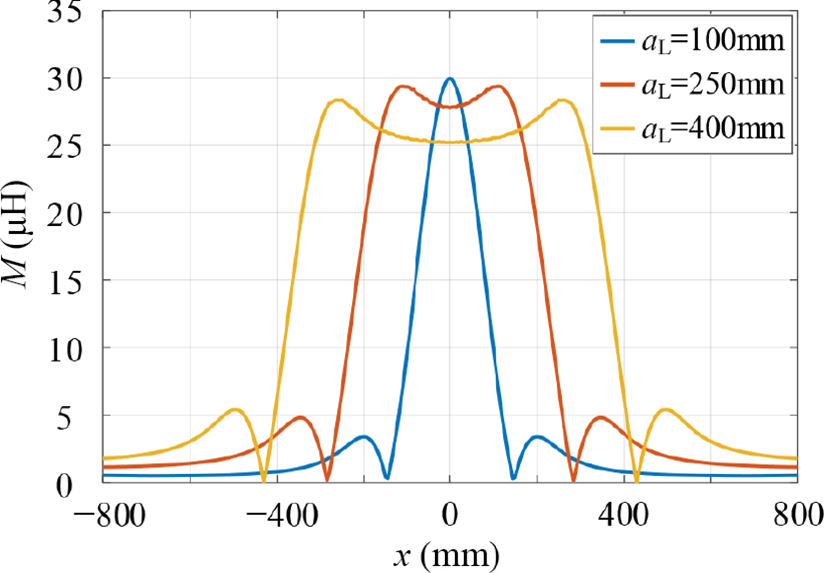
Figure 9.
Change of M as a function of the position of the Rx coil (with different length of the Tx coil in the X direction).
At the same time, the change in the curve in Fig. 9 also shows that when P reaches around (aL, 0, z3), the mutual inductance will decrease to near 0 due to the effective and ineffective magnetic flux cancellation, and at this point, the system cannot transfer energy. Even though a portion of the mutual inductance will quickly recover, the secondary side will still have a significant impact on the power transfer characteristics when approaching this point. Therefore, it is necessary to use a multi-channel power transfer method to compensate for the fluctuation of mutual inductance.
Output power fluctuation of the CLC-S compensated SISO and DISO system
-
Assuming that the Tx coils are arranged closely in pairs between each other, the SISO system is similar to Fig. 1. During the operation of an EV, only the nearest Tx coil in a straight-line distance to the Rx coil participates in power transmission, and any other Tx coil beyond this distance is considered to be outside the effective power supply area. The communication delay of the relative position sensor between the Rx coil and the Tx coil and the possible power interruption in the conduction of the Tx coil are ignored. When the input voltage u1 = 400 V, load resistance is 25 Ω, the original side compensation inductance Lft is set to 60 μH, and the Rx coil moves from x = −800 mm to x = 800 mm, the fluctuation curve of its output power is shown in Fig. 10.
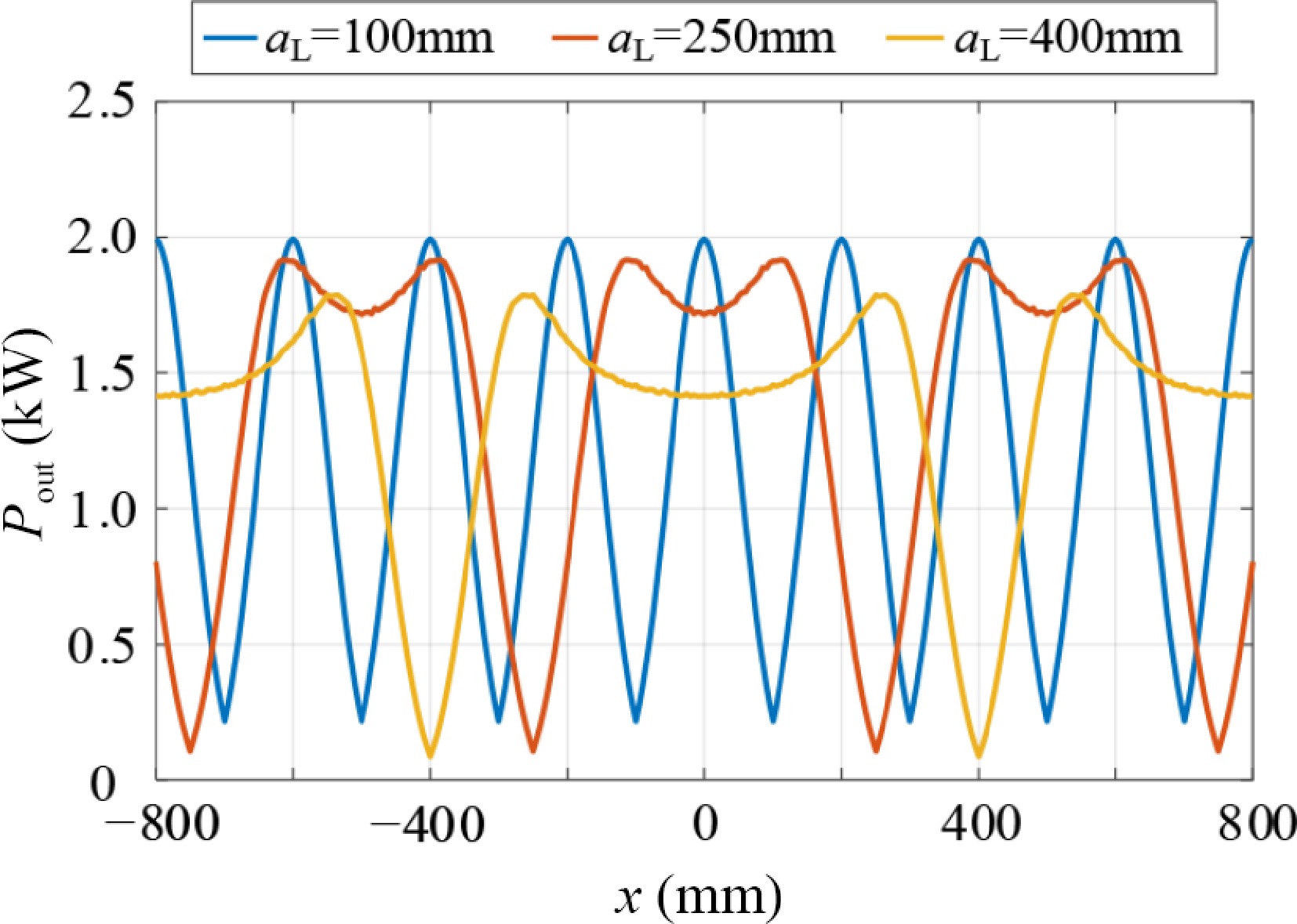
Figure 10.
Fluctuation curve of the output power.
It can be seen that, although longer Tx coils in the X direction help to reduce the power fluctuation within the effective coupling area, it is still unable to avoid the power dropping near 0. With the pre-fetched circuit parameters unchanged, the output power fluctuation as the EV moves of the CLC-S compensated DISO and SISO systems, of which the aL are set to 100 and 250 mm, are respectively shown in Figs 11 and 12.
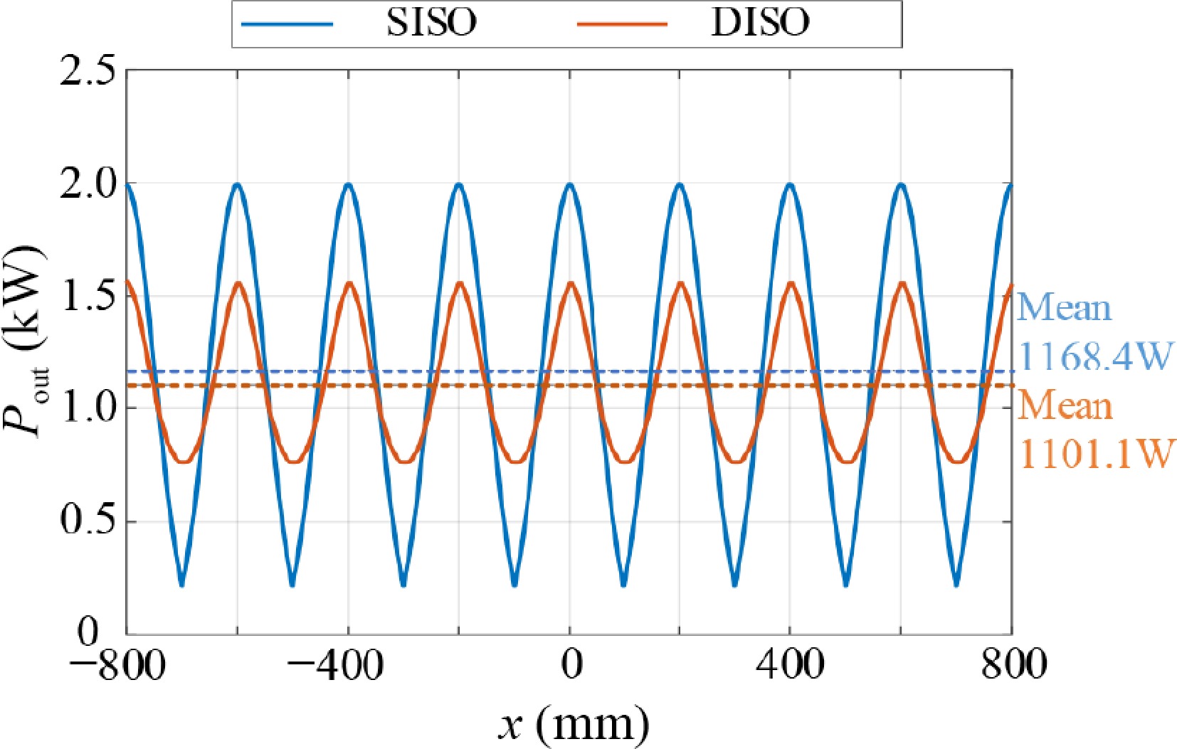
Figure 11.
Fluctuation curve of the output power of the CLC-S compensated SISO and DISO system ($ {a}_{\mathrm{L}}=100\text{ mm}) $.
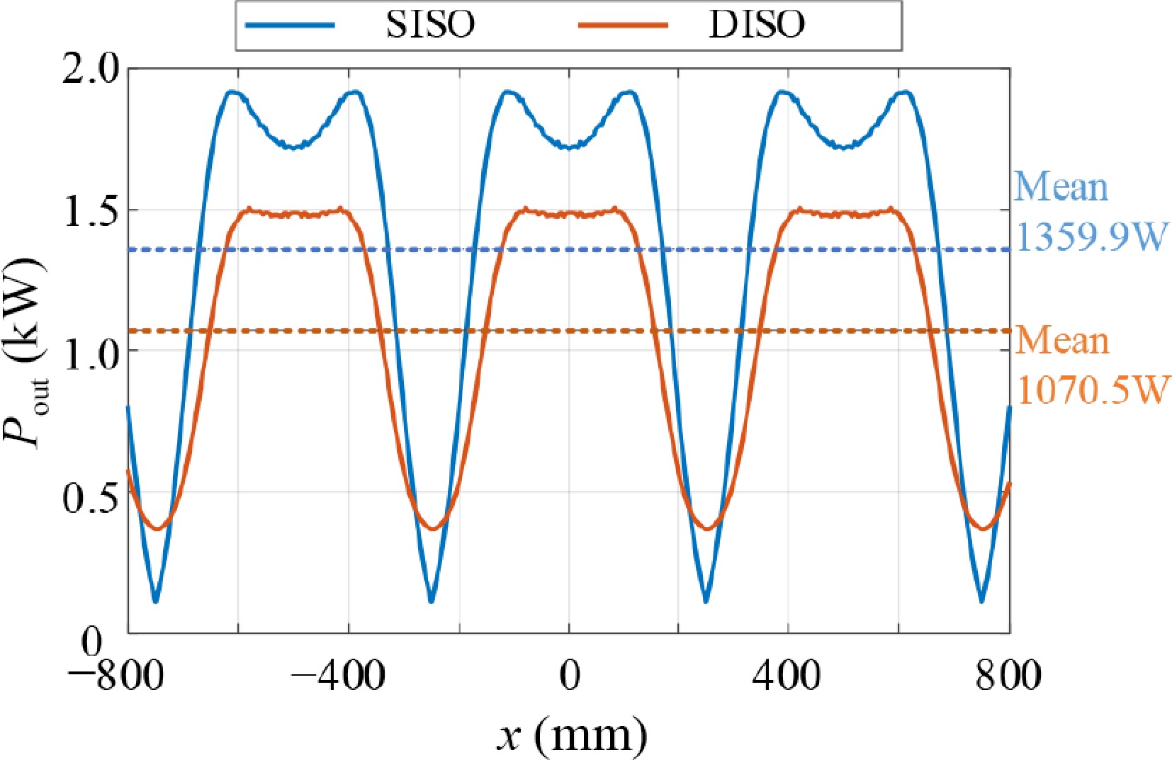
Figure 12.
Fluctuation curve of the output power of the CLC-S compensated SISO and DISO system (aL = 250 mm).
It can be seen that, without adding any material, the DISO system does reduce the output power fluctuation. Specifically, when aL = 100 mm, the output power fluctuation rate decreases to 54.52%, and when aL = 250 mm, the output power fluctuation rate decreases to 36.92%. However, for the average transmission power, it is hardly affected when aL = 100 mm, but decreases when aL = 250 mm.
The reason is that no matter what type of Tx coil is used, there is a decrease in mutual inductance to 0 near the array joint, followed by a rebound due to the exchange of effective and ineffective magnetic induction directions. However, from Fig. 8, it can be seen that when aL = 100 mm, the mutual inductance near the joint of the Tx coil array rebounds to around 4.81 μH, which is weaker than that to 3.37 μH when aL = 250 mm. It indicates that when designing the Tx coil array, it is necessary to fully consider the magnetic field superposition effect formed by the adjacent two coils in order to effectively leverage the advantages of coil shape and multi-channel power transmission.
Optimization design of the DISO magnetic coupler
-
According to the analysis in previous section, it can be seen that the design of the magnetic coupling coil has a significant impact on the stability of the system output power when using the DISO system. This section focuses on the superposition of the magnetic field during the switching process of the Tx coil, and aims to achieve a more stable output power by designing the magnetic coupling coil to counteract the end effects between adjacent coils.
The influence of the superposition of magnetic fields on mutual inductance
-
According to the principle of magnetic field superposition, when the Tx coils of the DISO system carry currents of the same frequency and phase, their magnetic effects can directly superimpose. In the previous section, for the same Rx coil and the same air gap, the use of a Tx coil with aL = 250 mm can balance the stability of mutual inductance and electromagnetic safety. Therefore, this section takes aL = 250 mm as an example to study the superposition effect of the magnetic field in the DISO DWPT system. For a magnetic coupler coupling a single Tx coil to an Rx coil, its mutual inductance curve simulated by ANSYS Maxwell is shown in Fig. 13. Unlike Fig. 8, when discussing the superposition effect, the mutual inductance has negative values.
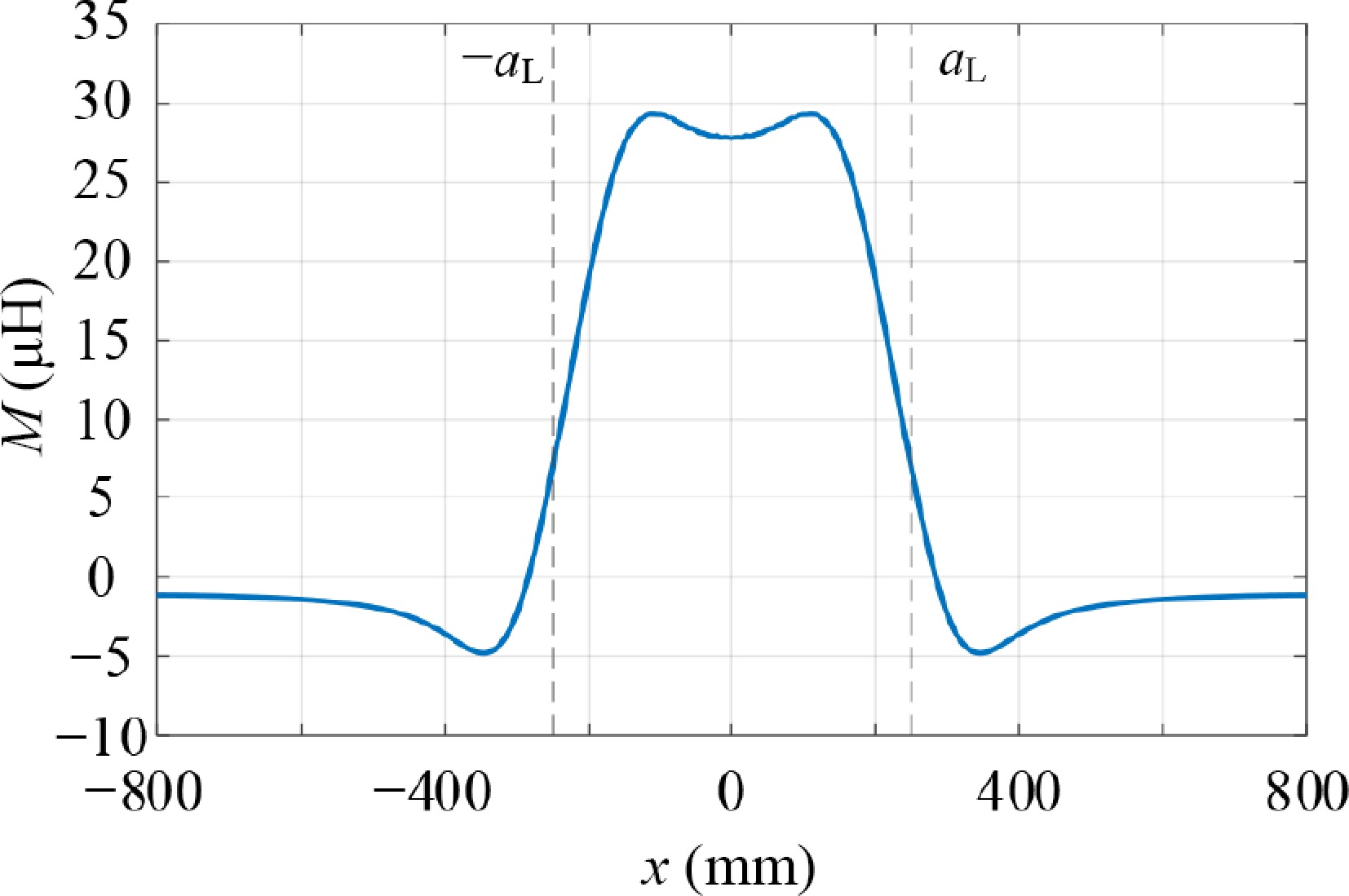
Figure 13.
The mutual inductance value considering the directionality of the magnetic field (aL = 250 mm).
To obtain the expression of mutual inductance superposition for multiple coils, the expression for a single Tx coil is first analyzed. It is assumed that the curve in Fig. 12 is a part of a periodic function M(x), and the function is fitted by a Fourier series for a part of x belonging to [−800, 800]. Generally, the Fourier series can be expressed as:
$ {M}_{0}\left(x\right)=\dfrac{{a}_{0}}{2}+\sum\limits_{n=1}^{\mathrm{\infty }}{a}_{n}\cos \left(\omega x\right)+{b}_{n}\sin \left(\omega x\right) $ (20) where, M0 represents the Tx coil with its center position at point 0, referred to as the 0 coil, and the coefficients can be calculated as:
$ \left\{\begin{aligned} &{a}_{n}=\dfrac{2}{T}\int\limits_{{x}_{0}}^{{x}_{0}+T}{M}_{0}\left(x\right)\cos \left(n\omega x\right)dx\\ &{b}_{n}=\dfrac{2}{T}\int\limits_{{x}_{0}}^{{x}_{0}+T}{M}_{0}\left(x\right)\sin \left(n\omega x\right)dx \end{aligned} \right.$ (21) The initial value of ω is set to 2π/1,600. By comparing the fitting situation from the 1st order to the 10th order, the Fourier series of the curve in Fig. 13 is obtained.
The root mean square value of the difference between the fitted and the simulated mutual inductance is shown in Table 2. The graphs of the Fourier series for each order and the simulated mutual inductance curve are plotted in Fig. 14. It can be observed that after reaching the 7th order, the improvement in the fitting effect is not significant with the increase in order. Therefore, the 7th order Fourier series is selected to fit the M0(x). The coefficients obtained in Eq. (22) are shown in Table 3.
Table 2. Root mean square values of the Fourier series of different orders.
Order Root mean square value Order Root mean square value 1 5.34 2 2.86 3 1.17 4 0.66 5 0.38 6 0.25 7 0.10 8 0.08 9 0.06 10 0.06 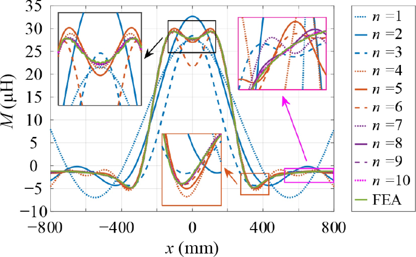
Figure 14.
Fitting situation of Fourier series of different orders.
Table 3. 7th order fourier series coefficients.
Symbol Value Symbol Value a0 7.827 a1 1.129 a2 1.148 a3 9.223 × 10⁻² a4 −0.7381 a5 −0.5092 a6 1.439 × 10⁻² a7 0.1055 b1 1.413 × 10⁻¹⁷ b2 −1.750 × 10⁻¹⁸ b3 1.198 × 10⁻¹⁶ b4 2.669 × 10⁻¹⁸ b5 1.864 × 10⁻¹⁷ b6 2.497 × 10⁻¹⁷ b7 −8.257 × 10⁻¹⁸ ω 4.102 × 10⁻³ For the superposition of magnetic fields from multiple coils, the corresponding mutual inductance expression can be directly obtained using the coordinate system shift operation of the transmitting coil, and can be expressed as:
$ {M}_{i}\left(x\right)=\dfrac{{a}_{0}}{2}+\sum\limits_{n=1}^{7}{a}_{n}\cos \left(\omega \left(x-{\varphi }_{i}\right)\right)+{b}_{n}\sin \left(\omega \left(x-{\varphi }_{i}\right)\right) $ (22) Mi(x) represents the mutual inductance formed between the i-th Tx coil and the Rx coil, with
$\varphi_i $ $\varphi_i $ $\varphi_i $ $\varphi_i $ $ {M}^{\prime}=\begin{cases} {M}_{i}+{M}_{i-1} \;\;\;x\in \left[-{\varphi }_{i},0\right)\\ {M}_{i}+{M}_{i+1}\;\;\; x\in \left[0,{\varphi }_{i}\right] \end{cases} $ (23) where, i−1 represents the coil behind the i-th coil (the position that EV first passes through). As the vehicle moves, its charging i-th coil also changes. It can be considered that Eq. (25) represents a new 'period', where the period T has changed to 2
$\varphi_i $ $\varphi_i $ 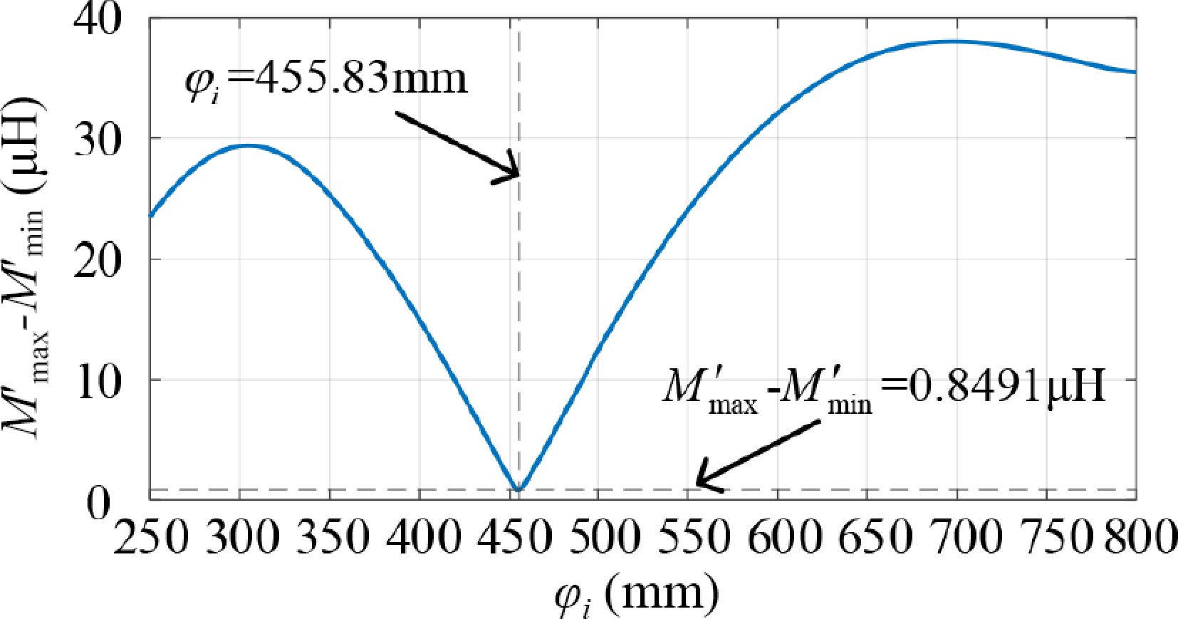
Figure 15.
Fluctuation amplitude of mutual inductance at different $\varphi _i $.
It can be observed that with the increase of
$\varphi_i $ $\varphi_i $ Evaluation system for multi-coil superposition
-
In the actual application process, output power fluctuation may not be the sole factor determining the design of the DWPT system's magnetic coupler. In the design process, other factors such as average output power and cost-effectiveness also need to be considered.
The time for the vehicle to be effectively coupled to a single Tx coil is short, so the total energy transmitted by a single coil is the main point of comparison. Under identical external circuit conditions, Fig. 16 represents the calculated total energy transmitted within the range of
$ x\in [-800,800] $ $\varphi_i $ 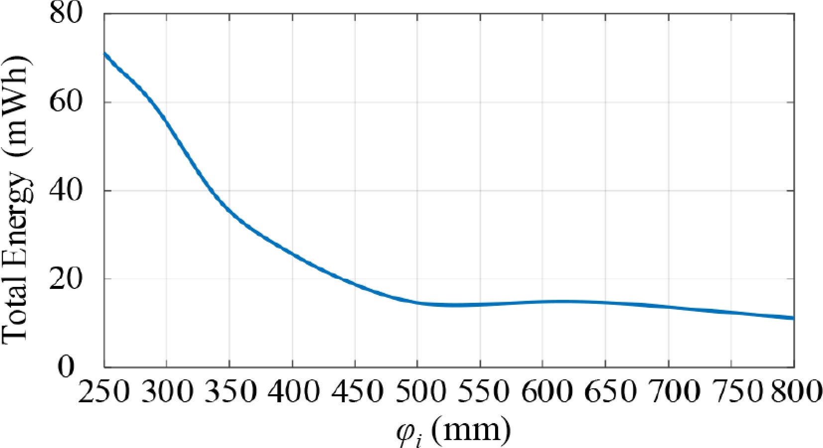
Figure 16.
Total energy transmission curve of the DWPT system under different $\varphi _i $.
As can be seen, during the process of vehicles traveling at a constant speed through this section, the total energy available to the vehicle decreases overall as
$ {\varphi }_{i} $ $\varphi_i $ However, for different
$\varphi_i $ $ {\rho }_{t}=\dfrac{2{a}_{\text{L}}}{{\varphi }_{i}}\times 100\text{% } $ (24) The higher the original side density, the more coils and ground power supply equipment are used, and the worse the economy.
The Figure of Merit (FOM) is proposed to comprehensively evaluate the DISO DWPT system, which combines the original side density index, total energy, and mutual inductance fluctuation level, defined as:
$ {\text{FOM}}_{\mathrm{i}}=\dfrac{{E}_{i}{}^{A}}{\rho _{i}^{C}\cdot {\left({{{M}^{\prime}}}_{\max }-{{{M}^{\prime}}}_{\min }\right)}^{B}} $ (25) In Eq. (25), Ei represents the total energy transmitted by the current power transfer device when a vehicle travels at a constant speed through a certain area. A, B, and C are the weighting coefficients for total energy, mutual inductance fluctuation, and original side density, respectively.
The determination of the weighting coefficients A, B, and C in the comprehensive FOM, as shown in Eq. (25), is based on the hierarchical design objectives of the system. Specifically, the coefficients are assigned as A = 2, B = 1, and C = 1 to reflect the critical priority structure. Since effective energy transfer is a fundamental prerequisite for any DWPT system, the total energy term (E) is assigned a dominant weight (A = 2). Meanwhile, the mutual inductance fluctuation and primary-side economy are treated as necessary constraints, with equal weights assigned (B = 1, C = 1). Based on this weighting scheme, the optimal design point is determined. Although a smaller center-to-center distance (e.g.,
$\varphi $ $\varphi $ $ i $ 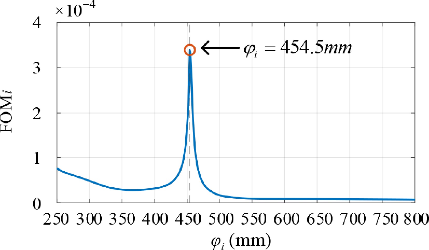
Figure 17.
The curve of FOMi as a function of $\varphi _i $.
When the value of A is twice that of the other two coefficients, the FOM is maximized at
$\varphi _i $ $\varphi _i $ 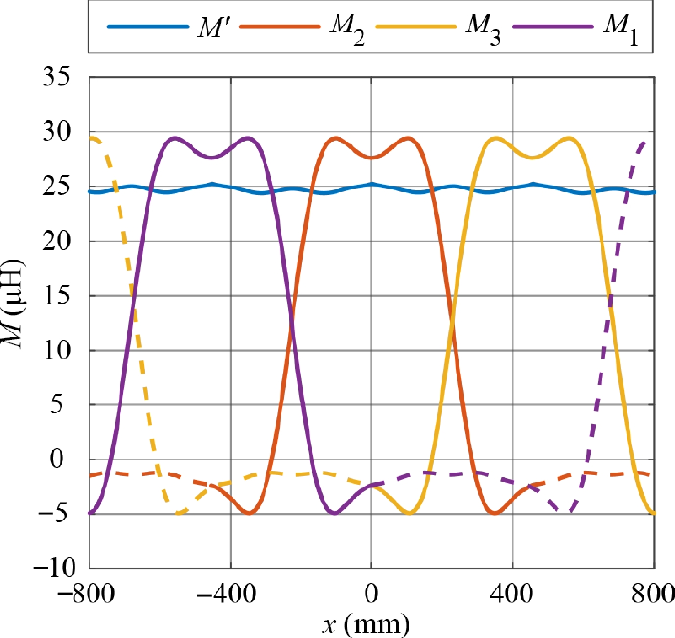
Figure 18.
The mutual inductance fluctuation curve.
In Fig. 18, the solid line represents the coil in operation, while the dashed line represents the coil that has been disconnected. It can be observed that the total mutual inductance M' remains stable throughout the movement compared to the fluctuation of M1, M2, M3. As for the output power in Fig. 18, when
$\varphi _i $ Based on the preceding analysis, a general design procedure for double-channel wireless charging systems can be summarized as follows:
(1) Select the initial system parameters and calculate the required mutual inductance (Meq). Then, based on this value and considering practical application scenarios, design and screen primary coil parameters that not only meet the Meq requirement but also maintain high mutual inductance over a wide range.
(2) Establish the continuous fluctuation model of the mutual inductance as described by Eq. (20). Adjust the center-to-center distance between adjacent Tx coil units, compute the variation in mutual inductance fluctuation with respect to this distance using Eq. (23), and determine the optimal center distance that minimizes the fluctuation.
(3) A figure of merit (FOM) is calculated through Eq. (24) by incorporating mutual inductance fluctuation, primary-side density, and the total energy transferred per road section, for further refinement of the optimal Tx coil center distance.
(4) Based on the input characteristics at the optimal center distance, assess soft-switching achievement under the design conditions and finalize the system design by fine-tuning the compensation capacitances with the guidance of Eq. (19).
This design procedure is summarized in Fig. 19.
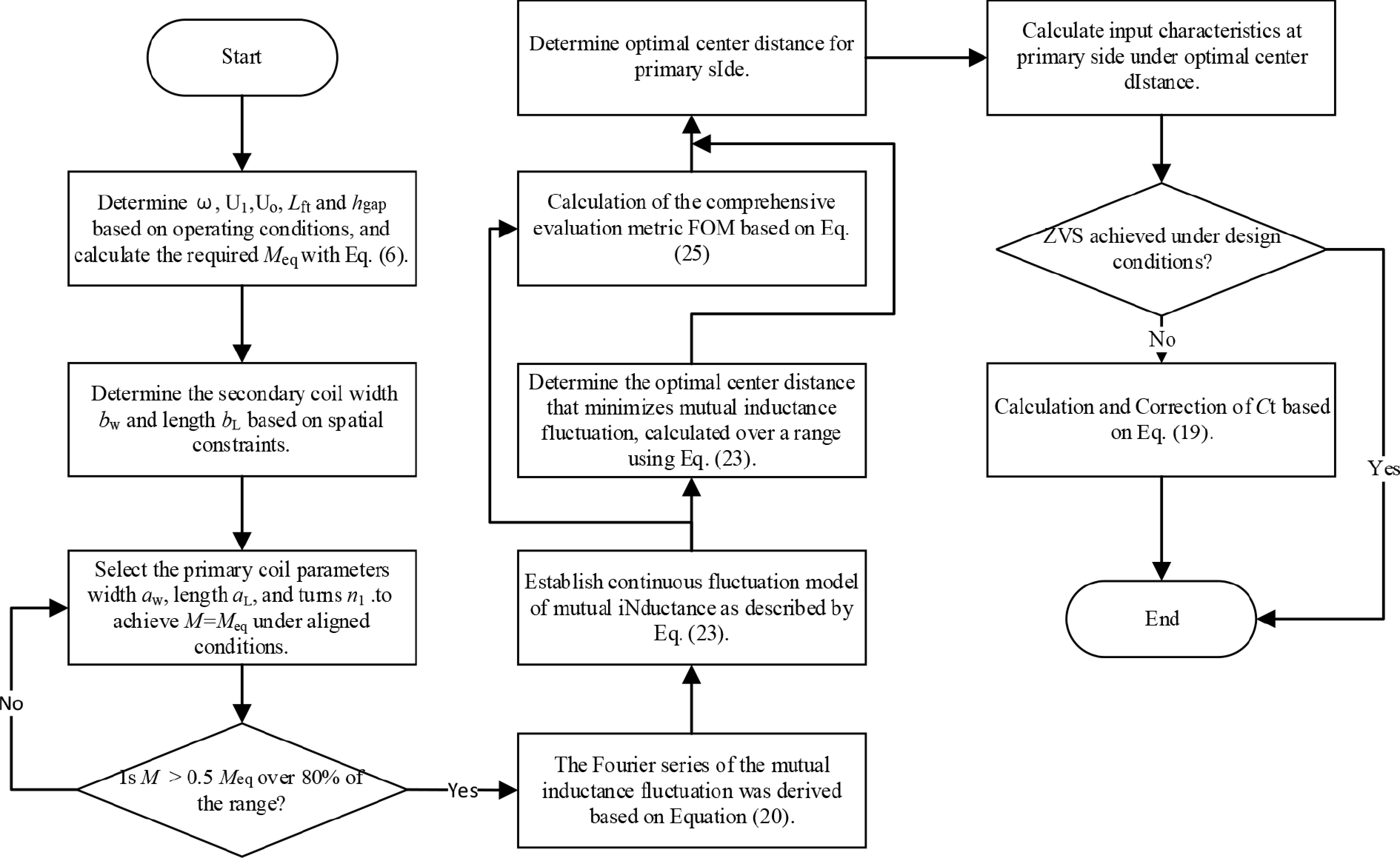
Figure 19.
Design flow of a double-channel WPTS.
-
To verify the effectiveness of the proposed method of topological design and center distance selection in suppressing output power fluctuations, FEA simulations and experiments were designed. An FEA model of multiple overlapping Tx coils was established in ANSYS Maxwell, with some design parameters shown in Table 4 (refer to Fig. 7 for symbols in the table). The magnetic coupler FEA model is shown in Fig. 20.
Table 4. Magnetic coupler design parameters.
Symbol Value Symbol Value t1 2 mm bL 100 mm t2 12 mm bW 100 mm aL 250 mm n2 15 αw 100 mm hgap 90 mm n1 15 $\varphi _i $ 455 mm 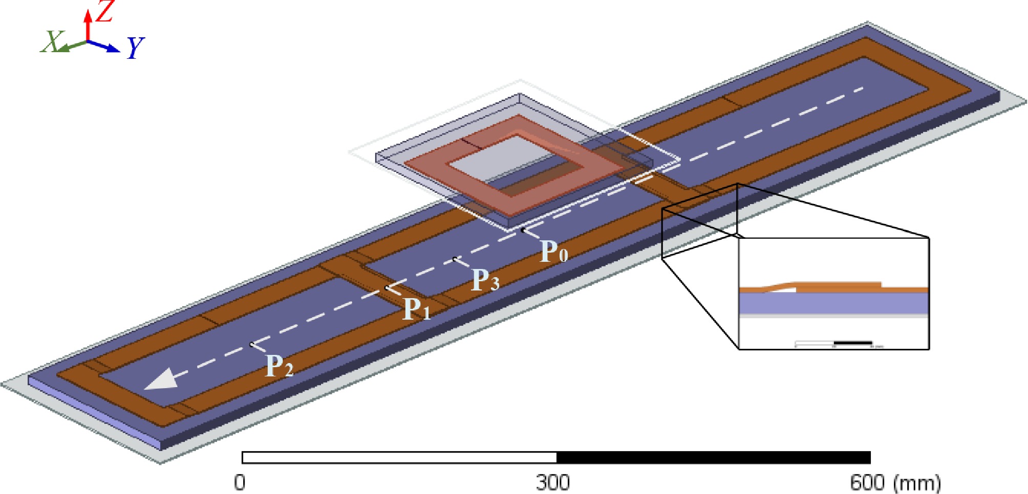
Figure 20.
DISO system magnetic coupler FEA model.
The physical experiment followed the same method as the FEA simulation. The magnetic coupler and test bench are shown in Fig. 20. To display the transmitting coils, a partial top-view photo is added in the upper right corner of the figure.
To safely and accurately control the relative motion of the Tx and Rx coils, as well as record continuous changes in the secondary-side output waveform, a three-axis electric control test platform was used to construct the experimental setup for the DWPT system. Since it is not possible to infinitely extend the array of Tx coils in the laboratory, the complete fluctuation cycle is simulated by folding back on the guide rail, that is, using
$ x\in [0,455] $ $ x\in [-455,455] $ In Fig. 21, the Tx coil is inverted on the tempered glass plate of the test platform, and the Rx coil is located on the movable base with an air gap of 90 mm. The coordinate system refers to the coordinate system of the magnetic coupling model in Fig. 1, with the center point of the Tx coil 2 located directly above the origin. In the experiment, the entire secondary side, except for the electronic load, starts from P1(455, 0, 1.5), travels at a constant speed of 0.2 m/s to P0(0, 0, 1.5), and then immediately returns to P1 at the same speed, simulating the vehicle's movement process.
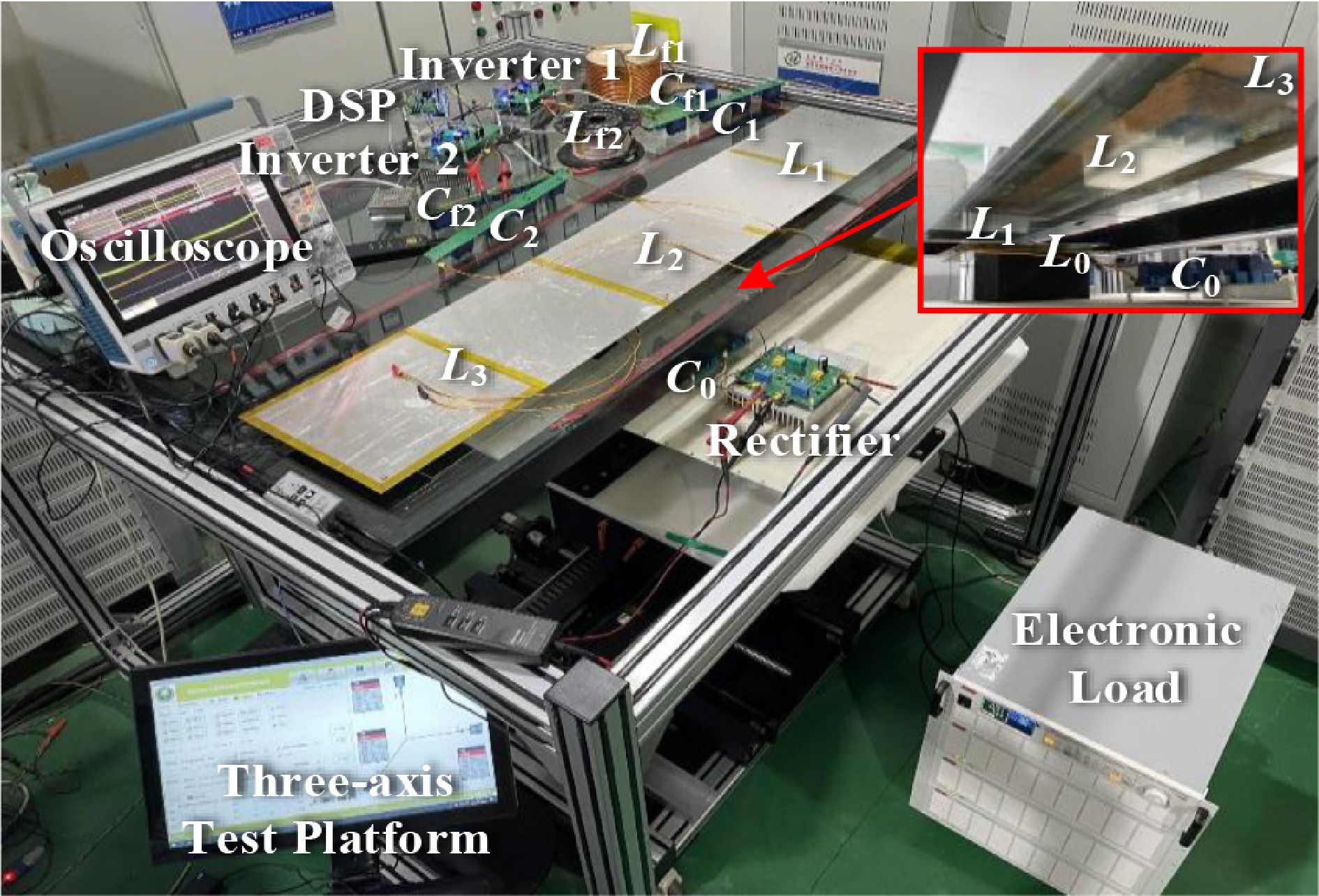
Figure 21.
Laboratory setup of the proposed DWPT system.
The full-bridge inverter is based on CREE silicon carbide power MOSFET, model C3M0040120D, and the full-bridge rectifier is based on CREE silicon carbide Schottky diode, model C5D50065D. An NGI N68144-1000-120 electronic load is used to simulate the equivalent resistance load of the vehicle power battery.
Firstly, the HIOKI IM3536 LCR meter is used to measure the inductance of the magnetic coupler at position P0. The simulation and physical inductance parameters of the magnetic coupler are compared in Table 5. It can be observed that the simulated inductance value and the measured value are relatively consistent, so the FEA calculation method adopted in the article is feasible and effective. Several important external circuit parameters are shown in Table 6.
Table 5. Comparison of simulated and actual electrical parameters of the magnetic coupler.
Description FEA Measurement Self-inductance of Tx coil 1 L1 230.86 μH 222.16 μH Self-inductance of Tx coil 2 L2 231.03 μH 226.54 μH Self-inductance of Tx coil 3 L3 230.75 μH 225.49 μH Self-inductance of Rx coil 0 L0 105.26 μH 101.68 μH Same side mutual inductance M12 −20.63 μH −20.91 μH Same side mutual inductance M23 −20.83 μH −21.82 μH Cross-coupling mutual inductance M01 −2.96 μH −3.53 μH Cross-coupling mutual inductance M02 26.39 μH 26.09 μH Cross-coupling mutual inductance M03 −2.91 μH −3.65 μH Table 6. Some important external circuit parameters.
Symbol Value Symbol Value f 85 kHz C1 13.44 nF R0 25 Ω C2 13.42 nF Lf1 58.62 μH C3 13.42 nF Lf2 60.01 μH Cf1 58.80 nF Lf3 59.95 μH Cf2 58.43 nF C0 34.04 nF Cf3 58.48 nF Figure 22 displays waveforms of inverter output currents and voltages at points P0, P1, and P2, with point locations labeled in Fig. 20. Experimental results in Fig. 22a and c validate the analytical model: when the Rx coil aligns with either Tx channel, the opposing Tx channel generates counter-directional currents to compensate for input current fluctuations.
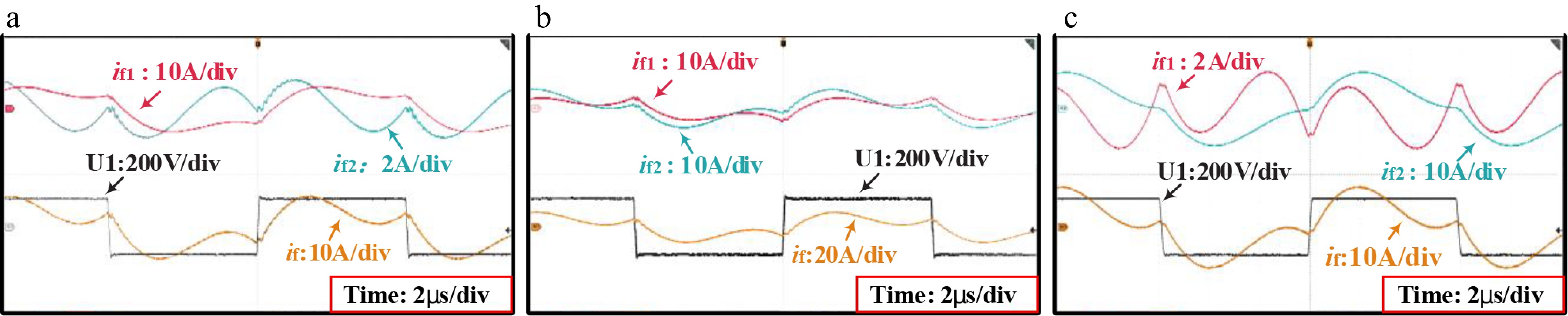
Figure 22.
Current and voltage waveforms at two characteristic positions during dynamic motion. (a) Position P0 (0.0, 1.5), (b) position P1 (227.5, 0, 1.5), (c) position P1 (455, 0, 1.5).
Figure 23 compares experimental measurements and theoretical calculations of MOSFET turn-off currents at three representative points. The measured results demonstrate excellent agreement with analytical predictions. At an input voltage U1 = 200 V, the MOSFET turn-off current If_off sustains robust ZVS operation throughout the dynamic process (minimum If_off = 4.4 A), consistently exceeding the ZVS critical threshold.

Figure 23.
Experimental and theoretical calculation results of the MOSFETs turn-off current If_ off.
Under the condition of a DC input voltage of 200 V and an output load of 25 Ω, the entire secondary side, except for the electronic load, is programmed to move at a constant speed from point P1 to point P0, immediately reverse back to point P1. The input and output variations of the CLC-S compensated SISO and simple stacked DISO DWPT systems are shown in Fig. 24a and b, respectively.
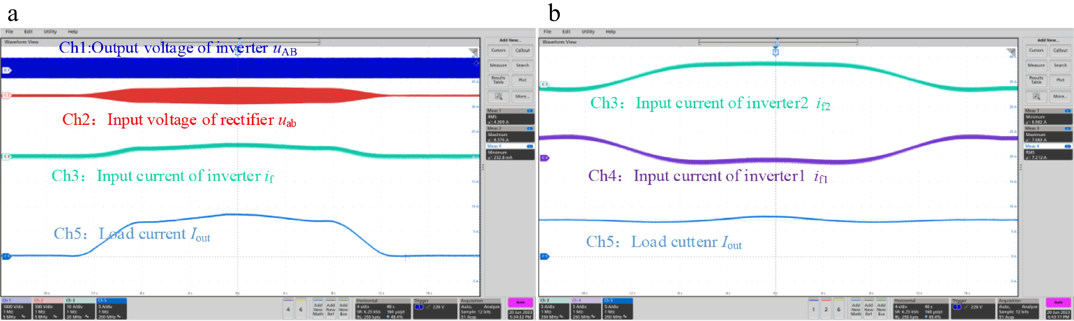
Figure 24.
Output power fluctuation waveforms of CLC-S compensated DWPT system: (a) SISO, (b) DISO.
When adjusting the position of the secondary side, the change of input current iCf1 follows the expected trend of initially increasing and then decreasing, which closely matches the measured mutual inductance fluctuation curve.
In the CLC-S compensated SISO system, the maximum output current is 8.58 A, corresponding to an output power of 1.84 kW, and the minimum output current is 0.23 A. The average output power throughout the entire movement process is 1.22 kW. When using the DISO system, as shown in 0, it is evident that the fluctuation amplitude of the output current has been effectively suppressed. Throughout the entire movement process, the maximum output current is 7.68 A, corresponding to an output power of 1.48 kW, and the minimum output current is 6.98 A, with a minimum output power of 1.22 kW. The average output power is 1.30 kW, and the output fluctuation amplitude has been reduced to 0.26 kW, accounting for 20.00% of the average output power. Although the usage of primary-side materials has increased by 9.89%, the average output power has increased by 6.58%, and the output power fluctuation has been reduced by 85.87%.
To further evaluate the energy characteristics of the system, the DC-DC efficiency curves of the SISO and DISO systems vs the receiver position x are compared in Fig. 25. As observed, the efficiency of the SISO system degrades rapidly as the receiver deviates from the alignment position, dropping to 71.2% at x = 200 mm. Beyond this range, the mutual inductance falls into a dead zone where the coupling is insufficient to maintain stable power flow; consequently, efficiency data is not recorded. In contrast, the proposed DISO system maintains a robust efficiency profile, fluctuating only slightly between 91.1% and 92.5%. It is worth noting that this efficiency trend is consistent with the equivalent mutual inductance (M′) curve shown in Fig. 18. This consistency demonstrates that the proposed overlapping coil structure and CLC-S compensation successfully mitigate the adverse effects of cross-coupling and misalignment, ensuring high-efficiency operation across the entire charging zone.
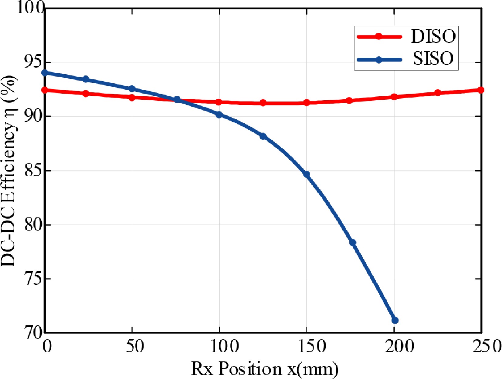
Figure 25.
Comparison of the measured DC-DC efficiency curves between the SISO and DISO systems vs receiver position x.
Figure 26 illustrates the detailed power loss distribution, with a calculated total loss of 107.02 W. The energy dissipation is mainly distributed among the magnetic coupler and power semiconductors. Notably, coil copper loss (25%) and ferrite core loss (19%) represent the dominant loss factors, which align with the inherent characteristics of loosely coupled systems. In addition, the inverter MOSFETs and rectifier diodes contribute 22% and 18% to the total loss, respectively. The consistency between the calculated loss and the measured efficiency (approx. 92%) further confirms the validity of the experimental data.
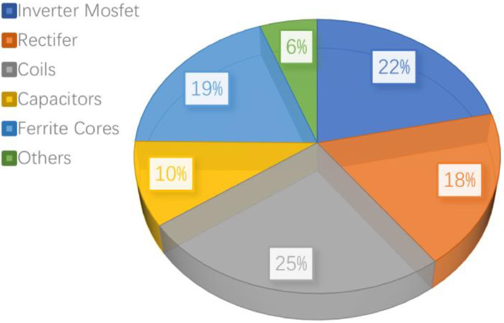
Figure 26.
Loss distribution of the DISO prototype.
-
This study proposes a DISO circuit architecture based on CLC-S compensation to mitigate output power fluctuations in dynamic wireless power transfer systems with arrayed transmitting coils. Theoretical analysis reveals that suppressing equivalent mutual inductance fluctuations constitutes the core requirement for stabilizing output power. Through parameter sensitivity analysis, the series compensation capacitance (Ct) of the Tx coil is identified as a parameter decoupled from the system output power. An adaptive Ct tuning strategy is developed based on ZVS boundary conditions, effectively mitigating cross-coupling effects induced by overlapping structures. To ensure dynamic stability, a systematic optimization framework is established by combining Fourier-series modeling with a Figure of Merit evaluation. This approach enables the precise mathematical determination of the optimal center distance for universal overlapping arrays, replacing empirical de-sign with analytical rigor. Experimental validation is conducted via a 1.3 kW prototype, demonstrating complete ZVS operation throughout dynamic charging processes under specified conditions. Compared to SISO systems, the proposed DISO system achieves a 6.58% increase in average output power while reducing power fluctuations by 85.87%.
-
The authors confirm contributions to the paper as follows: study conception and design: Li W, Deng J, Han Y; data collection: Han Y, Wang W; analysis and interpretation of results: Han Y, Wang W; draft manuscript preparation: Li W, Deng J, Han Y. All authors reviewed the results and approved the final version of the manuscript.
-
The data that support the findings of this study are available upon request from the corresponding author.
-
This work was supported by the National Natural Science Foundation of China (Grant No. 52207232).
-
The authors declare that they have no conflict of interest.
- Copyright: © 2026 by the author(s). Published by Maximum Academic Press, Fayetteville, GA. This article is an open access article distributed under Creative Commons Attribution License (CC BY 4.0), visit https://creativecommons.org/licenses/by/4.0/.
-
About this article
Cite this article
Li W, Han Y, Deng J, Wang W. 2026. Adaptive CLC-S tuned DWPT system with overlapping coil magnetic coupler for output power fluctuation mitigation. Wireless Power Transfer 13: e016 doi: 10.48130/wpt-0026-0006 

Adaptive CLC-S tuned DWPT system with overlapping coil magnetic coupler for output power fluctuation mitigation
- Received: 15 October 2025
- Revised: 23 December 2025
- Accepted: 27 January 2026
- Published online: 04 June 2026
Abstract: In dynamic wireless power transfer (DWPT) systems employing transmitting (Tx) coil arrays, output power fluctuations aggravate battery charging current ripples and compromise system stability. To address this issue, this work proposes a CLC-S compensation topology based on a dual-input single-output (DISO) architecture along with a cooperative coil design methodology. Theoretical analysis of the DISO CLC-S compensation network reveals that equivalent mutual inductance fluctuation is the main cause of output power instability, and that cross-coupling between Tx coils can disrupt the zero-voltage-switching (ZVS) condition. Parameter sensitivity analysis identifies the Tx coil series compensation capacitance as the key tunable parameter decoupled from the system output power. Based on the ZVS boundary condition, a tuning strategy is proposed to suppress the cross-coupling effect. To minimize equivalent mutual inductance fluctuations, an analytical model for the mutual inductance between the receiving (Rx) coil and adjacent dual transmit (Tx) coils under lateral movement is proposed. The model enables the determination of the optimal center-to-center distance between Tx coils, and supports the design of an overlapping Tx coil layout. A 1.3 kW prototype is developed for validation. Test results demonstrate that, compared to a single-input single-output (SISO) system, the proposed solution reduces output power fluctuation by 85.87%, while full ZVS operation during dynamic charging is achieved. In this case, the average output power has been increased by 6.58%.
-
Key words:
- DWPT /
- ZVS /
- EV /
- Magnetic coupler /
- Output power fluctuation mitigation