


-
Generally, to ensure the high efficiency and safety of charging, the typical charging algorithm of electric bicycle onboard battery packs is first constant current (CC) and then constant voltage (CV). In order to design a WPT system that complies with the above-mentioned charging algorithm, three traditional closed-loop control methods of phase shift control[1−3], frequency conversion control[4−6], and DC–DC assistive control[7−9] are adopted. However, the above three control methods all increase the complexity of the system controller design.
The hybrid topology switching method, is extensively studied for its simplicity of control. Various authors[10−15] propose multiple types of hybrid topologies to realize CC and CV charging characteristics. However, additional passive components, AC switches, and corresponding driving circuits are unavoidable in hybrid topologies, which increases the complexity of the circuit structure.
Nowadays, as an alternative, the dual-frequency switching method is gaining popularity. Previous researchers[16−21] present various types of dual-frequency switching methods to achieve CC and CV charging characteristics. However, since some standard frequency recommendations such as from 79 to 90 kHz in the SAEJ2954 standard from the Society of Automotive Engineers, it is difficult to tune circuit parameters to meet actual application requirements.
In addition, the three methods mentioned above have to rely on additional detection circuits and communication links to determine the timing of CC-CV transition. To prevent the risk of accidental load open-circuit in CC mode, it is essential to add open-circuit protection circuits in the above-mentioned methods. Committed to the further optimization of CC and CV WPT systems, this manuscript proposes an LCC-S compensated WPT system to realize inherent CC and CV characteristics and automatic CC-CV transition function. Complicated control, cumbersome circuit structure, difficult-to-adjust parameters, and expensive detection circuits, communication links, open-circuit protection circuits can be avoided, so the proposed system is robust, simple, and low-cost. The proposed system is preferentially recommended for low and medium-power charging applications such as electric bicycles.
-
The overall circuit structure of the proposed WPT system is depicted in Fig. 1. This structure can be seen as a cascade of a clamp circuit composed of diodes D1, D2, and a special LCC-S compensation WPT system. E is the DC input voltage. For the convenience of analysis, the components in the topology are recorded as LR, LS, LP, CR, CP, and CS respectively. The mutual inductance of LS and LP is denoted as M. UAO and UBO are the AC output voltages from the clamp circuit and the half-bridge inverter, respectively. The equivalent AC resistance of the part surrounded by the blue dotted line is expressed as RE and satisfies the relation RE = 2RB/π2. There are three operating modes for the clamp circuit: the turned-off mode, the partly activated mode, and the fully active mode, and these three modes correspond to CC mode, CC-CV transition process, and CV mode respectively. The analysis of the different modes is given as follows:

Figure 1.
Overall circuit structure of the proposed WPT system and circuit structure of the WPT system working in CV mode.
Analysis of CC mode
-
At the initial stage of charging, since
$ \sqrt 2 \left| {{{U}_{AO}}} \right| \leqslant E $ 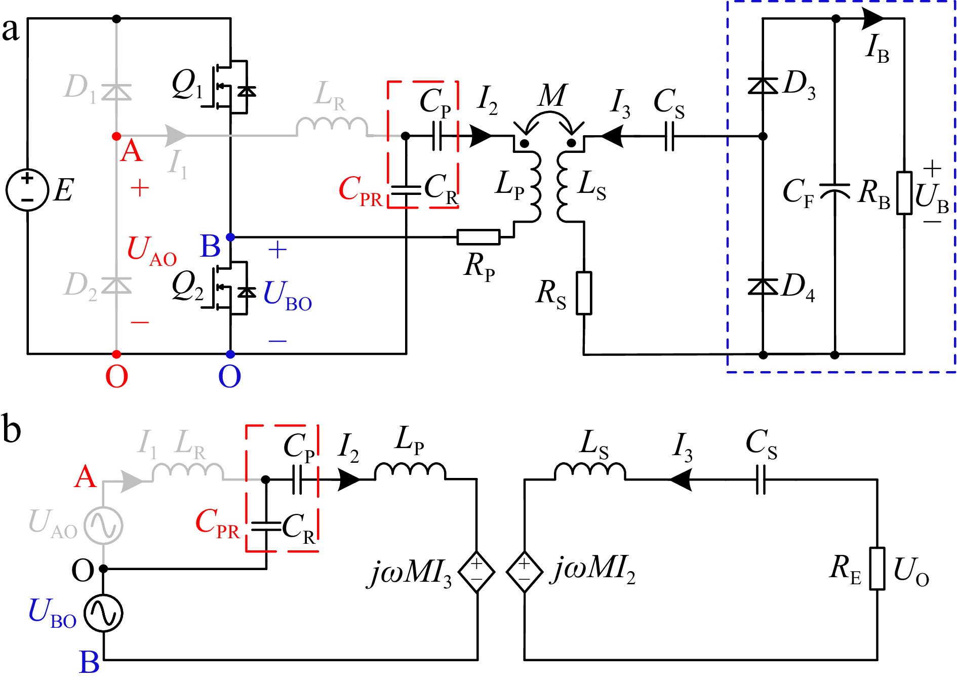
Figure 2.
Circuit structure and equivalent circuit of the WPT system working in CC mode. (a) Circuit structure diagram. (b) Equivalent circuit diagram.
$ \left\{ {\begin{array}{*{20}{l}} {{U_{BO}} = \left(j\omega {L_P} + \dfrac{1}{{j\omega {C_{PR}}}}\right){I_2} + j\omega M{I_3}{\text{ }}} \\ {0 = \left(j\omega {L_S} + \dfrac{1}{{j\omega {C_S}}} + {R_E}\right){I_3} + j\omega M{I_2}{\text{ }}} \end{array}} \right. $ (1) For simplicity of analysis, it is assumed that all compensation capacitors are fully compensated at a fixed angular frequency ω. The compensation relationships are as follows:
$ j\omega {L_P} + \dfrac{1}{{j\omega {C_{{\text{PR}}}}}} = 0,j\omega {L_{\text{S}}} + \dfrac{1}{{j\omega {C_{\text{S}}}}} = 0 $ (2) Combining Eqns (1) & (2), RE = 2RB/π2 and
$ {I_B} = (\sqrt 2 /{\text π}){I_3} $ $ {I_B} = \dfrac{{2E}}{{{{\text π} ^2}\omega M}},\;{Z_{in}} = \dfrac{{{U_{BO}}}}{{{I_2}}} = \dfrac{{{\omega ^2}{{\text π} ^2}{M^2}}}{{2R_B^2}} $ (3) It can be known from Eqn (3), the input impedance Zin is purely resistive and the charging current IB is independent of load resistance.
Analysis of CC-CV transition process
-
When
$ E\leqslant\sqrt{2}\left|{U}_{\text{AO}}\right|\leqslant(4/{\text π} )E $ $ \sqrt 2 \left| {{U_{AO}}} \right| $ $ \sqrt 2 \left| {{U_{AO}}} \right| $ Analysis of CV mode
-
With the continuous increase of
$ \sqrt 2 \left| {{U_{AO}}} \right| $ $ (4/{\text π})E\leqslant\sqrt{2}\left|{U}_{AO}\right| $ For the clamp circuit composed of D1 and D2, the relationship between the RMS value of the output voltage UAO and the input voltage E is
$ {U_{AO}} = (\sqrt 2 /{\text π})E $ $ {U_{BO}} = (\sqrt 2 /{\text π})E $ The equivalent circuit in CV mode is displayed in Fig. 3. According to KVL, Eqn (4) can be obtained.
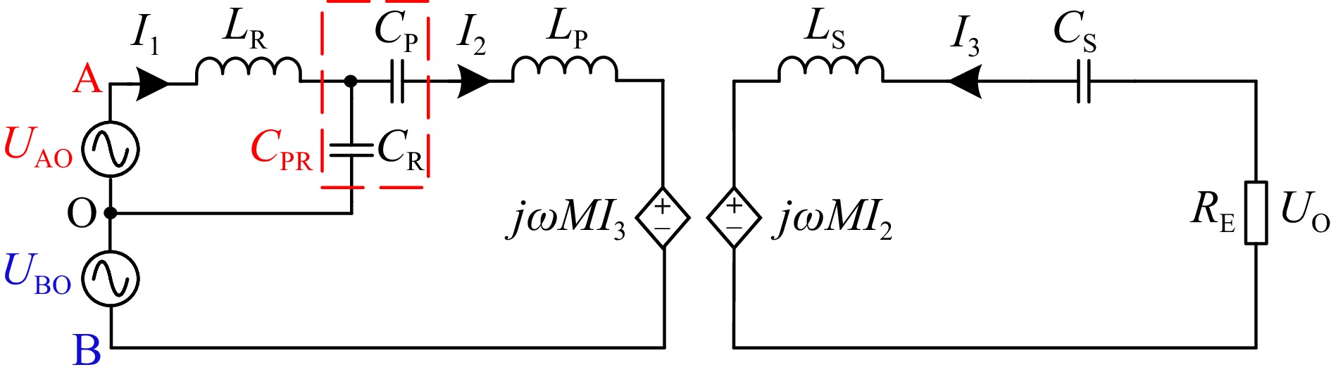
Figure 3.
Equivalent circuit of the WPT system working in CV mode.
$ \left\{ {\begin{array}{*{20}{l}} {{U_{AO}} = \left(j\omega {L_R} + \dfrac{1}{{j\omega {C_R}}}\right){I_1} - \dfrac{1}{{j\omega {C_R}}}{I_2}{\text{ }}} \\ {{U_{BO}} = \left(j\omega {L_P} + \dfrac{1}{{j\omega {C_{PR}}}}\right){I_2} - \dfrac{1}{{j\omega {C_R}}}{I_1} + j\omega M{I_3}{\text{ }}} \\ {0 = \left(j\omega {L_S} + \dfrac{1}{{j\omega {C_S}}} + {R_E}\right){I_3} + j\omega M{I_2}{\text{ }}} \end{array}} \right. $ (4) Similar to the CC analysis process, Eqn (2) and jωLR + 1/jωCR = 0 need to be satisfied. Substituting Eqn (2), UAO = UBO and jωLR + 1/jωCR = 0 into Eqn (4), Eqn (5) can be deduced as:
$ {U_O} = - \dfrac{{M{U_{AO}}}}{{{L_R}}},\;{Z_{in}} = \dfrac{{{U_{BO}}}}{{{I_2}}} = - \omega {L_R}{\text{ }} $ (5) where, UO is the equivalent AC input voltage of the rectifier.
According to
$ {U_O} = (\sqrt 2 /{\text π}){U_B} $ ${U_{AO}} = (\sqrt 2 /{\text π})E $ $ {U_B} = \dfrac{M}{{{L_R}}}E $ (6) Equations (5) & (6) prove that the system can achieve load-independent CV output and ZPA operation.
-
Given an electric bicycle battery pack with a nominal voltage of 60 V and a capacity of 10 Ah, an experimental prototype with 2 A/66 V charging outputs was fabricated, as shown in Fig. 4. The operating frequency f was set as 85 kHz and the input DC voltage E as 100 V. According to Eqns 1/CPR = 1/CP + 1/CR, (2), (3), (6) and jωLR + 1/jωCR = 0, the parameters of each compensation component can be calculated, as listed in Table 1.
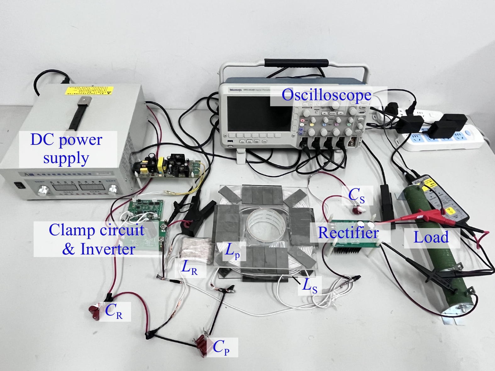
Figure 4.
Experimental prototype.
Table 1. Specific compensation parameters of the proposed system.
Parameters Value CP, CS, CR (nF) 175.4, 175.4, 175.4 LP, LS, LR, M (μH) 50, 50, 28.5, 19.2 Experimental results
-
Experimental waveforms for CC mode, CC-CV transition, and CV mode were captured, as shown in Fig. 5. Figure 5a & b show the experimental waveforms in CC mode at RB = 10 and 15 Ω, respectively. IB maintains at a constant value of 2 A and I1 is null. Figure 5c & d display that the clamp circuit is partially activated, and the branch where L2 is located generates discontinuous I1 during the CC-CV transition process. In CV mode, the clamp circuit is fully activated, the current I1 is continuous, UB maintains at a constant value of 66 V and the relevant waveforms are shown in Fig. 5e & f. Furthermore, the phases of the input voltage UBO and the input current I2 are consistent in the three modes, the proposed system can achieve ZPA operation throughout the charging process.

Figure 5.
Experimental waveforms. (a) RB = 5 Ω. (b) RB = 10 Ω. (c) RB = 30 Ω. (d) RB = 40 Ω. (e) RB = 100 Ω. (f) RB = 150 Ω.
Figure 6 shows the trends of IB (represented in red), UB (represented in blue), and charging efficiency (represented in purple) during the charging process. It can be obtained that when
$ \sqrt{2}\left|{U}_{AO}\right|\leqslant E $ $ (4/{\text π})E\leqslant \sqrt{2}\left|{U}_{AO}\right| $ 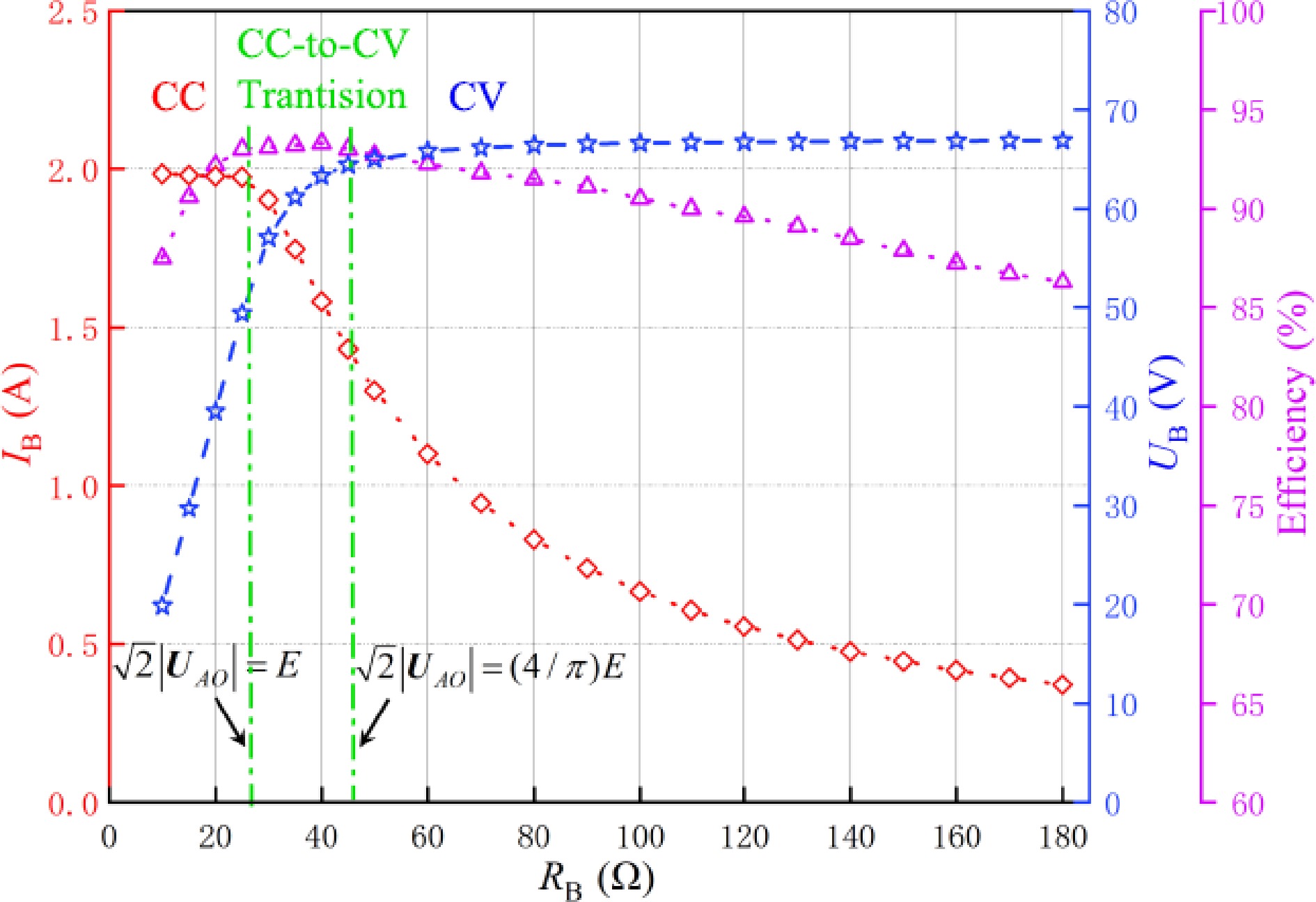
Figure 6.
Measured IB, UB, and efficiency curve vs RB.
-
The current study proposes a special LCC-S compensated WPT system with inherent CC and CV output characteristics and automatic transition from CC to CV charging mode. In the initial stage of the charging, the CC mode can be realized through the SS structure. As charging proceeds, when the voltage peak on the clamp circuit satisfies
$ (4/{\text π})E\leqslant\sqrt{2}\left|{U}_{AO}\right| $ This work was supported in part by the Natural Science Foundation of Hunan Province (Grant No. 2024JJ7186), in part by the Key Laboratory of Small and Micro Intelligent Agricultural Machinery Equipment and Application of Hunan Province Education Department of China (Grant No. SJT012), and in part by the Institute of Image Information Processing and Intelligent Control of Hunan University of Science and Engineering (Grant No. XKY008).
-
The authors confirm contribution to the paper as follows: conceptualization, resources, funding acquisition, writing-original draft preparation, writing-review and editing: Zhou X; methodology, data curation: Zhou X, Tan Y; software: Zhou X, Tan Y, Wang L; validation: Chen A, Yang L; formal analysis: Tan Y, Wang L; Investigation, project administration: Chen A; visualization: Wang L, Chen A; supervision: Yang L. All authors have read and agreed to the final version of the manuscript.
-
All data generated or analyzed during this study are included in this published article.
-
The authors declare that they have no conflict of interest.
- Copyright: © 2024 by the author(s). Published by Maximum Academic Press, Fayetteville, GA. This article is an open access article distributed under Creative Commons Attribution License (CC BY 4.0), visit https://creativecommons.org/licenses/by/4.0/.
-
About this article
Cite this article
Zhou X, Tan Y, Wang L, Chen A, Yang L. 2024. A special LCC-S compensated WPT system with inherent CC-CV transition for electric bicycles charging. Wireless Power Transfer 11: e013 doi: 10.48130/wpt-0024-0011 

A special LCC-S compensated WPT system with inherent CC-CV transition for electric bicycles charging
- Received: 13 August 2024
- Revised: 11 October 2024
- Accepted: 15 October 2024
- Published online: 03 December 2024
Abstract: The charging algorithm of first constant current (CC) and then constant voltage (CV) is popular for electric bicycle onboard battery packs. This manuscript proposes an LCC-S compensated wireless power transfer (WPT) system to realize inherent CC and CV characteristics and automatic CC-CV transition function. During charging, the proposed system can operate in SS tank for CC charging and LCC-S tank for CV charging, respectively. Unlike the previous closed-loop control, hybrid topology switching, and dual-frequency switching methods, the proposed method has an automatic CC-CV transition function due to the special circuit structure. The detection circuits, communication links, and open-circuit protection circuits are omitted, and the system's receiver conforms to the minimalist design principle. Therefore, the proposed system is low-cost, robust, and simple. A confirmatory experimental prototype is fabricated to verify the correctness and effectiveness of the proposed system.